


 Trouble in Your Tank: Implementing Direct Metallization in Advanced Substrate Packaging
 It’s Only Common Sense: Storytelling That Sells—Stop Pitching, Start Painting Pictures
 The Right Approach: Get Ready for ISO 9001 Version 6


Scientists Revisit Optical Constants of Ultrathin Gold Films
October 18, 2017 | MIPTEstimated reading time: 3 minutes
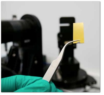
Researchers at Moscow Institute of Physics and Technology (MIPT) have conducted highly precise measurements of the optical constants of ultrathin gold films with thicknesses ranging from 20 to 200 billionths of a meter in the optical part of the electromagnetic spectrum. Thin gold films are key components of modern micro- and nanoscale optical and optoelectronic devices. The research findings will be in demand among researchers in the field. The paper was published in the journal Optics Express ("Optical constants and structural properties of thin gold films").
Metal films with a thickness of tens of nanometers, or tens of billionths of a meter, are widely used to produce compact chemical and biological sensors, photodetectors, solar cells, and components for optical computers. When nanofilms are made thinner than 10 nanometers, they become not just conductive but also flexible and transparent, which might be applicable in a variety of modern devices.
Gold, which is widely used in nanoscale device development, has proved to be the most suitable metal for the purpose. Such applications require gold in the form of very thin films or nanostructures. To develop and optimize devices, precise data on the properties of such films are necessary. But most of the data used by researchers at present are reported in papers published almost half a century ago.
For instance, one of the most frequently cited articles on the optical constants of gold is "Optical constants of the noble metals" by P.B. Johnson and R.W. Christy, published as early as 1972. The Scopus citation database reveals that the reference constants for gold from this paper have been used in at least 10,000 other publications. To appreciate the significance of this work, it is important to keep in mind that in the 70s, research into the optical properties of thin metal films required a tremendous effort, because the challenging experiments had to be followed by complex calculations and computers were not yet widespread.
Thinner is better
State-of-the-art laboratory equipment and the nearly unlimited computing power available to modern researchers enable more detailed studies of thin metal films. However, it is known that the optical properties of such films -- and therefore the efficiency of devices based on them -- depend on factors such as film thickness, deposition rate, and the temperature of the substrate used for film deposition.
Accordingly, the MIPT researchers adjusted the initial conditions, namely the deposition rate and the substrate temperature, so as to optimize the optical properties of the film. After that, they conducted the necessary measurements by means of spectroscopic ellipsometry, X-ray diffractometry, electron and atomic force microscopy. The data obtained allowed the MIPT team to study in detail how the properties of thin gold films are related to their structure and average grain size.
The structure of a material affects its physical properties to a large extent, because it is at grain boundaries that conduction electrons are scattered, losing energy -- the way a ball in a pinball machine loses its momentum as it runs into obstacles. As it turned out, both optical losses and direct current resistivity are substantially increased, as the thickness of the gold film is reduced to below 80 nanometers.
The authors of the paper provide reference data on the optical constants of gold for a wide range of wavelengths, from 300 to 2,000 nanometers, for films that are 20 to 200 nanometers thick. These findings will be of use to researchers working on various nanophotonic devices and metamaterials.
State-of-the-art technology
To grow thin films, the researchers used a technique called electron beam evaporation, which involves the following steps:: A purified silicon substrate is introduced into a vacuum chamber. Opposite the substrate, a metal sample is positioned. The metal, in this case gold, is then subjected to a beam of electrons accelerated by an electric field. This rapidly heats up the gold causing it to melt and eventually transform into vapor. The evaporated gold atoms are then transported across a region of low pressure from their source and undergo condensation on the substrate to form the thin film.
"Provided that you maintain a high vacuum, heat the metal appropriately, and otherwise follow the procedure, this technique yields films of arbitrary thickness, which is determined by the evaporation time. Moreover, the films are almost perfectly smooth, having a roughness of less than a nanometer," comments Valentyn Volkov, who heads the Laboratory of Nanooptics and Plasmonics at MIPT. "Such films can be used in optics and optoelectronics to develop high-sensitivity compact biosensors, solar cells, broadband photodetectors, and optoelectronic computer components." Gold films of this kind with a thickness of about 40 nanometers are already used in biosensor design.
Share on:


Testimonial
"We’re proud to call I-Connect007 a trusted partner. Their innovative approach and industry insight made our podcast collaboration a success by connecting us with the right audience and delivering real results."
Julia McCaffrey - NCAB GroupSuggested Items
Trouble in Your Tank: Implementing Direct Metallization in Advanced Substrate Packaging
09/15/2025 | Michael Carano -- Column: Trouble in Your TankDirect metallization systems based on conductive graphite are gaining popularity throughout the world. The environmental and productivity gains achievable with this process are outstanding. Direct metallization reduces the costs of compliance, waste treatment, and legal issues related to chemical exposure. A graphite-based direct plate system has been devised to address these needs.
Curtiss-Wright Selected by Rheinmetall to Provide Turret Drive Stabilization System for the KF51 Panther Main Battle Tank
08/11/2025 | BUSINESS WIRECurtiss-Wright announced it has been selected by Rheinmetall Landsysteme Germany (RLS) to provide its modular turret drive stabilization system (TDSS) technology in support of the KF51 Panther Main Battle Tank (MBT).
European Global Mobile Artillery Rocket System Launcher Proves Capability with First-Ever Firing
08/04/2025 | Lockheed MartinLockheed Martin and Rheinmetall, partners in the Global Mobile Artillery Rocket System (GMARS) program, successfully conducted the first live fire of the GMARS launcher, demonstrating its capability to launch GMLRS rockets.
Rheinmetall Expands Local Production Activities in Romania
07/28/2025 | RheinmetallRheinmetall has established a comprehensive local production network in Romania, encompassing both its own companies in the country and new partnerships with Romanian companies.
STMicroelectronics, Metalenz Sign a New License Agreement to Accelerate Metasurface Optics Adoption
07/14/2025 | STMicroelectronicsSTMicroelectronics, a global semiconductor leader serving customers across the spectrum of electronics applications and Metalenz, the pioneer of metasurface optics, announced a new license agreement.