


 Trouble in Your Tank: Implementing Direct Metallization in Advanced Substrate Packaging
 It’s Only Common Sense: Storytelling That Sells—Stop Pitching, Start Painting Pictures
 The Right Approach: Get Ready for ISO 9001 Version 6


Deep-Depletion: A New Concept for MOSFETs
October 27, 2017 | AIP.orgEstimated reading time: 4 minutes
Silicon has provided enormous benefits to the power electronics industry. But performance of silicon-based power electronics is nearing maximum capacity.
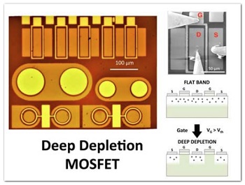
Left: Optical microscope image of the MOSCAPs and diamond deep depletion MOSFETs (D2MOSFETs) of this work. Top right: Scanning electron microscope image of a diamond D2MOSFET under electrical investigation. S: Source, G: Gate, D: Drain. Bottom right: D2MOSFET concept. The on-state of the transistor is ensured thanks to the accumulation or flat band regime. The high mobility channel is the boron-doped diamond epilayer. The off-state is achieved thanks to the deep depletion regime, which is stable only for wide bandgap semiconductors. For a gate voltage larger than a given threshold, the channel is closed because of the deeply and fully depleted layer under the gate. (Image: Institut NÉEL)
Enter wide bandgap (WBG) semiconductors. Seen as significantly more energy-efficient, they have emerged as leading contenders in developing field-effect transistors (FETs) for next-generation power electronics. Such FET technology would benefit everything from power-grid distribution of renewable-energy sources to car and train engines.
Diamond is largely recognized as the most ideal material in WBG development, owing to its superior physical properties, which allow devices to operate at much higher temperatures, voltages and frequencies, with reduced semiconductor losses.
A main challenge, however, in realizing the full potential of diamond in an important type of FET -- namely, metal-oxide-semiconductor field-effect transistors (MOSFETs) -- is the ability to increase the hole channel carrier mobility. This mobility, related to the ease with which current flows, is essential for the on-state current of MOSFETs.
Researchers from France, the United Kingdom and Japan incorporate a new approach to solve this problem by using the deep-depletion regime of bulk-boron-doped diamond MOSFETs. The new proof of concept enables the production of simple diamond MOSFET structures from single boron-doped epilayer stacks. This new method, specific to WBG semiconductors, increases the mobility by an order of magnitude. The results are published this week in Applied Physics Letters ("Deep depletion concept for diamond MOSFET").
In a typical MOSFET structure, an oxide layer and then a metal gate are formed on top of a semiconductor, which in this case is diamond. By applying a voltage to the metal gate, the carrier density, and hence the conductivity, of the diamond region just under the gate, the channel, can be changed dramatically. The ability to use this electric "field-effect" to control the channel conductivity and switch MOSFETS from conducting (on-state) to highly insulating (off-state) drives their use in power control applications. Many of the diamond MOSFETs demonstrated to date rely on a hydrogen-terminated diamond surface to transfer positively charged carriers, known as holes, into the channel.
More recently, operation of oxygen terminated diamond MOS structures in an inversion regime, similar to the common mode of operation of silicon MOSFETS, has been demonstrated. The on-state current of a MOSFET is strongly dependent on the channel mobility and in many of these MOSFET designs, the mobility is sensitive to roughness and defect states at the oxide diamond interface where unwanted carrier scattering occurs.
To address this issue, the researchers explored a different mode of operation, the deep-depletion concept. To build their MOSFET, the researchers deposited a layer of aluminum oxide (Al2O3) at 380 degrees Celsius over an oxygen-terminated thick diamond epitaxial layer. They created holes in the diamond layer by incorporating boron atoms into the layer. Boron has one less valence electron than carbon, so including it leaves a missing electron which acts like the addition of a positive charge, or hole. The bulk epilayer functioned as a thick conducting hole channel. The transistor was switched from the on-state to the off-state by application of a voltage which repelled and depleted the holes -- the deep depletion region.
In silicon-based transistors, this voltage would have also resulted in formation of an inversion layer and the transistor would not have turned off. The authors were able to demonstrate that the unique properties of diamond, and in particular the large band gap, suppressed formation of the inversion layer allowing operation in the deep depletion regime.
"We fabricated a transistor in which the on-state is ensured by the bulk channel conduction through the boron-doped diamond epilayer," said Julien Pernot, a researcher at the NEEL Institute in France and an author of the paper. "The off-state is ensured by the thick insulating layer induced by the deep-depletion regime. Our proof of concept paves the way in fully exploiting the potential of diamond for MOSFET applications." The researchers plan to produce these structures through their new startup called DiamFab.
Pernot observed that similar principles of this work could apply to other WBG semiconductors. "Boron is the doping solution for diamond," Pernot said, "but other dopant impurities would likely be suitable to enable other wide bandgap semiconductors to reach a stable deep-depletion regime."
Share on:


Testimonial
"Advertising in PCB007 Magazine has been a great way to showcase our bare board testers to the right audience. The I-Connect007 team makes the process smooth and professional. We’re proud to be featured in such a trusted publication."
Klaus Koziol - atgSuggested Items
Rules of Thumb: Design007 Magazine, November 2024
11/11/2024 | I-Connect007 Editorial TeamRules of thumb are everywhere, but there may be hundreds of rules of thumb for PCB design. They’re built on design formulas, fabricators’ limitations, and tribal knowledge. And unfortunately, some longtime rules of thumb should be avoided at all costs. How do we separate the wheat from the chaff, so to speak?
Connect the Dots: Best Practices for Prototyping
09/21/2023 | Matt Stevenson -- Column: Connect the DotsPCB prototyping is a critical juncture during an electronic device’s journey from concept to reality. Regardless of a project’s complexity, the process of transforming a design into a working board is often enlightening in terms of how a design can be improved before a PCB is ready for full production.
The Drive Toward UHDI and Substrates
09/20/2023 | I-Connect007 Editorial TeamPanasonic’s Darren Hitchcock spoke with the I-Connect007 Editorial Team on the complexities of moving toward ultra HDI manufacturing. As we learn in this conversation, the number of shifting constraints relative to traditional PCB fabrication is quite large and can sometimes conflict with each other.
Asia/Pacific AI Spending Surge to Reach a Projected $78 Billion by 2027
09/19/2023 | IDCAsia/Pacific spending on Artificial Intelligence (AI) ), including software, services, and hardware for AI-centric systems will grow to $78.4 billion in 2027, according to International Data Corporation's latest Worldwide Artificial Intelligence Spending Guide.
Intel to Sell Minority Stake in IMS Nanofabrication Business to TSMC
09/13/2023 | IntelIntel Corporation announced that it has agreed to sell an approximately 10% stake in the IMS Nanofabrication business to TSMC. TSMC’s investment values IMS at approximately $4.3 billion, consistent with the valuation of the recent stake sale to Bain Capital Special Situations.