


 Trouble in Your Tank: Implementing Direct Metallization in Advanced Substrate Packaging
 It’s Only Common Sense: Storytelling That Sells—Stop Pitching, Start Painting Pictures
 The Right Approach: Get Ready for ISO 9001 Version 6


Optoelectronics Without Glass
November 7, 2017 | ETH ZurichEstimated reading time: 3 minutes
Researchers at ETH Zurich have developed the first opto-electronic circuit component that works without glass and is instead made of metal. The component, referred to as a modulator, converts electrical data signals into optical signals. It is smaller and faster than current modulators, and much easier and cheaper to make.
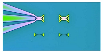
Microscopic image of a chip. Top left: functional modulator with electrical contacts; right: test modulator without electrical contact; below: test components. (Photograph: ETH Zurich)
Optical components for microelectronics must be made of glass. Metals are not suitable for this purpose, since optical data can propagate only across roughly a distance of 100 micrometres. This was the general view of scientists until recently. A team of researchers headed by Juerg Leuthold, professor in the Department of Information Technology and Electrical Engineering, has now succeeded in doing what was thought to be impossible and developed a light-processing component made of metal. The researchers have presented their findings in the latest issue of the journal Science.
They accomplished this feat by building a small enough component: at just 3 x 36 micrometres, it is within a size range in which both optical and electrical information can propagate in metals.
Component for fibre optic networks
The component is a modulator: modulators convert electrical data signals into optical signals. They are installed in modern internet routers used for fibre optic networks and enable fibre optic data connections between computer units in data centres. However, the standard components used today function differently than the new modulators.
The new component works by aiming the light from a fibre optic source at the modulator, causing the electrons on its surface to oscillate. Experts refer to this as a surface plasmon oscillation. This oscillation can be changed indirectly by electrical data pulses. When the oscillation of the electrons is converted back into light, the electrical information is now encoded onto the optical signal. This means that the information is converted from an electrical into an optical data pulse that can be transmitted via fibre optics.
Schematic representation of the metallic modulator: Left: a continuous beam of light strikes a metallic lattice that deflects the light onto the chip. Right: an optical data pulse exits the component. (Photograph: ETH Zurich)
Faster and smaller
Two years ago, Leuthold and his colleagues developed one of these plasmonic modulators (ETH News reported). At the time, it was the smallest and fastest modulator ever built, but the semiconductor chip still had various glass components.
By replacing all the glass components with metallic ones, the scientists have succeeded in building an even smaller modulator that works up to highest speed. “In metals, electrons can move at practically any speed, whereas the speed in glass is limited due to its physical properties,” says Masafumi Ayata, a doctoral student in Leuthold’s group and lead author of the study. In the experiment, the researchers succeeded in transmitting data at 116 gigabits per second. They are convinced that with further improvements, even higher data transfer rates will be possible.
Page 1 of 2
Share on:


Testimonial
"We’re proud to call I-Connect007 a trusted partner. Their innovative approach and industry insight made our podcast collaboration a success by connecting us with the right audience and delivering real results."
Julia McCaffrey - NCAB GroupSuggested Items
Trouble in Your Tank: Implementing Direct Metallization in Advanced Substrate Packaging
09/15/2025 | Michael Carano -- Column: Trouble in Your TankDirect metallization systems based on conductive graphite are gaining popularity throughout the world. The environmental and productivity gains achievable with this process are outstanding. Direct metallization reduces the costs of compliance, waste treatment, and legal issues related to chemical exposure. A graphite-based direct plate system has been devised to address these needs.
Closing the Loop on PCB Etching Waste
09/09/2025 | Shawn Stone, IECAs the PCB industry continues its push toward greener, more cost-efficient operations, Sigma Engineering’s Mecer System offers a comprehensive solution to two of the industry’s most persistent pain points: etchant consumption and rinse water waste. Designed as a modular, fully automated platform, the Mecer System regenerates spent copper etchants—both alkaline and acidic—and simultaneously recycles rinse water, transforming a traditionally linear chemical process into a closed-loop system.
Driving Innovation: Depth Routing Processes—Achieving Unparalleled Precision in Complex PCBs
09/08/2025 | Kurt Palmer -- Column: Driving InnovationIn PCB manufacturing, the demand for increasingly complex and miniaturized designs continually pushes the boundaries of traditional fabrication methods, including depth routing. Success in these applications demands not only on robust machinery but also sophisticated control functions. PCB manufacturers rely on advanced machine features and process methodologies to meet their precise depth routing goals. Here, I’ll explore some crucial functions that empower manufacturers to master complex depth routing challenges.
Trouble in Your Tank: Minimizing Small-via Defects for High-reliability PCBs
08/27/2025 | Michael Carano -- Column: Trouble in Your TankTo quote the comedian Stephen Wright, “If at first you don’t succeed, then skydiving is not for you.” That can be the battle cry when you find that only small-diameter vias are exhibiting voids. Why are small holes more prone to voids than larger vias when processed through electroless copper? There are several reasons.
The Government Circuit: Navigating New Trade Headwinds and New Partnerships
08/25/2025 | Chris Mitchell -- Column: The Government CircuitAs global trade winds continue to howl, the electronics manufacturing industry finds itself at a critical juncture. After months of warnings, the U.S. Government has implemented a broad array of tariff increases, with fresh duties hitting copper-based products, semiconductors, and imports from many nations. On the positive side, tentative trade agreements with Europe, China, Japan, and other nations are providing at least some clarity and counterbalance.