


 Trouble in Your Tank: Implementing Direct Metallization in Advanced Substrate Packaging
 It’s Only Common Sense: Storytelling That Sells—Stop Pitching, Start Painting Pictures
 The Right Approach: Get Ready for ISO 9001 Version 6


New Insights on 'Captured' Electrons Could Improve Flash Memory
November 8, 2017 | NISTEstimated reading time: 4 minutes
An entirely new model of the way electrons are briefly trapped and released in tiny electronic devices suggests that a long-accepted, industry-wide view is just plain wrong about the way these captured electrons affect the behavior of hardware components such as flash memory cells.
The model, devised by scientists at the National Institute of Standards and Technology (NIST), was tested to explain how electron capture and emission creates the insidious noise that increasingly threatens performance as electronic devices continue to shrink in size.
Those effects, variously known as burst noise, popcorn noise or random telegraph noise (RTN) “have become a major problem for extremely small devices,” said NIST researcher Kin Cheung, the lead author of a new report (link is external) in IEEE Transactions on Electron Devices.
Charge trapping is one of the known causes of flash memory failure. The new model, which NIST physicist John Kramar called “a major paradigm shift in charge-trapping modeling,” could lead to a different approach to manage this problem, and potentially, a new way of making the memory cells smaller.
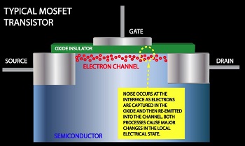
Typical MOSFET transistor
RTN noise consists of abrupt random drops in voltage or current caused by itinerant electrons that are briefly captured from, and then rejoin, the main flow along a current channel in, for example, a common type of transistor called a MOSFET.
“The effect was mostly negligible back in the good old days when devices were larger and there were lots of electrons flowing around,” Cheung said. But in today’s advanced devices, with feature dimensions in the range of 10 nanometers (nm, billionths of a meter) or less, the active area is so small that it can be swamped by a single trapped charge.
“As you get down to the very smallest sizes, RTN can be nearly 100 percent as strong as the signal you’re trying to measure,” Cheung said. “In those conditions, reliability disappears.”
In the case of RTN, the basics are known: The noise is caused by the action of electrons near the interface between two materials such as an insulator layer and the bulk of the semiconductor in a transistor. Specifically, an electron is pulled out of the current flow and trapped in a defect in the insulator; after a short time, it is emitted back into the main current in the semiconductor. What actually happens on the atomic scale at each stage of the process, however, is incompletely understood.
The orthodox approach to account for those effects is to treat all the trapped electrons as a single 2-D sheet of charge that extends uniformly across the center of the insulator. Each emitted electron is thought to return to the semiconductor in a reverse of the same process by which it was captured, causing very little change in the presumably stable state along the insulator/semiconductor boundary.
That model, when applied to very small devices, didn’t make sense to the NIST scientists. Among other difficulties, it ignored the fact that, once they are immobilized, electrons cause considerable distortions in local electrical field conditions along the boundary, affecting current flow. “We’re saying the traditional way doesn’t really work,” Cheung said. “You have to rethink this thing. The old model doesn’t make reasonable assumptions about how charge carriers behave.”
The researchers proposed a new model, based on local effects, in which the mechanisms of capture and emission are dramatically different from the standard picture. For one thing, they determined that quantum mechanics, the modern theory that describes the behavior of these systems, makes it hugely improbable, if not impossible, for electrons to get out of the insulator the same way they got in.
“It’s like a highway where there is an exit ramp, but there’s no on ramp,” says NIST co-author Jason Campbell. “You can go in, but you can’t come back that way. You’ve got to come back a different way. That is, there is a set of rules for capture that don’t apply to emission.”
“When you realize that the capture and emission processes are decoupled,” Cheung said, “you quickly have a very different view of the problem.”
The standard RTN picture supposes a weak interaction of trapped charge with its local surroundings―in this case, the highly separated electric charge in the silicon dioxide that often makes up the insulator layer in a transistor. NIST scientists found that a weak interaction is inconsistent with known physics and not in agreement with reports from two independent laboratories. Indeed, the interaction energy of a captured electron can be more than 10 times greater than previously believed. Recognition of this stronger interaction energy enables the new local field picture to explain RTN naturally.
The success of the new model, and the resulting drastic change in the understanding of both capture and emission, suggested that many long-held ideas would have to be thoroughly reconsidered.
“That was a very scary, very unsettling conclusion,” Campbell said. “I mean, this is tear-up-the-textbook stuff.”
The researchers hope the new model will help chip engineers and designers understand in much greater detail how devices degrade, and what will be required to get to the next stage of miniaturization while maintaining reliability and reducing noise.
Share on:


Testimonial
"We’re proud to call I-Connect007 a trusted partner. Their innovative approach and industry insight made our podcast collaboration a success by connecting us with the right audience and delivering real results."
Julia McCaffrey - NCAB GroupSuggested Items
Alternative Manufacturing, Inc. (AMI) Announces Commitment to Excellence in Industrial, Defense, Aerospace, Renewables, and Robotics Markets
09/16/2025 | Alternative Manufacturing, Inc.Alternative Manufacturing, Inc. (AMI), a 100% employee-owned contract manufacturer, proudly reaffirms its leadership in the electronics manufacturing services (EMS) industry with a continued commitment to delivering high-quality PCBAs and box builds across the industrial, defense, aerospace, renewable energy, and robotics markets.
Advint Incorporated Brings Artificial Intelligence to Electroplating Training
09/11/2025 | Advint IncorporatedAdvint Incorporated is introducing a new dimension to its electroplating training programs: the integration of Artificial Intelligence (AI). This initiative reflects the company’s commitment to providing PCB fabricators and manufacturers in the USA and Canada with training that is practical, forward-looking, and directly relevant to today’s production challenges.
Elementary Mr. Watson: Running the Signal Gauntlet
09/11/2025 | John Watson -- Column: Elementary, Mr. WatsonIf you’ve ever run a military obstacle course, you know it’s less “fun fitness challenge” and more “how can we inflict as much pain in the shortest time possible?” You start fresh—chest out, lungs full of confidence, thinking you might even look good doing this—and 10 seconds later, you’re questioning all your life choices.
It's Only Common Sense: The Evolution of Prospecting
09/08/2025 | Dan Beaulieu -- Column: It's Only Common SenseCold calling isn’t dead. I don’t care what the LinkedIn gurus or the TikTok “sales coaches” say. Picking up the phone and talking to another human being is still one of the fastest ways to grow your business. But (and it’s a big but), cold calling is different now. The world and buyers have changed. You can’t smile-and-dial like it’s 1987, reading the same tired script, hoping the gatekeeper is too bored to block you. If you’re still cold calling the old way—no research, relationship, or relevance—you’re showing up to a gunfight with a butter knife.
Elementary Mr. Watson: Routing Hunger Games—May the Traces Be Ever in Your Favor
08/26/2025 | John Watson -- Column: Elementary, Mr. WatsonI’d like to share a harsh truth, and I say this as a friend: PCB designers are often their own worst enemy. It’s rarely the complexity of the circuit, the last-minute changes from mechanical, the limited enclosure space, or the ever-expanding list of design rules that send projects to the dust heap of failed boards. More often, it's our own decisions, made too quickly and narrowly, and with too little foresight, that sabotage an otherwise good design.