


 Trouble in Your Tank: Implementing Direct Metallization in Advanced Substrate Packaging
 It’s Only Common Sense: Storytelling That Sells—Stop Pitching, Start Painting Pictures
 The Right Approach: Get Ready for ISO 9001 Version 6


Transfer Technique Produces Wearable GaN Gas Sensors
November 10, 2017 | Georgia TechEstimated reading time: 4 minutes
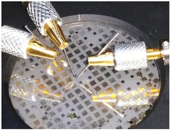
A transfer technique based on thin sacrificial layers of boron nitride (BN) could allow high-performance gallium nitride (GaN) gas sensors to be grown on sapphire substrates and then transferred to metallic or flexible polymer support materials. The technique could facilitate the production of low-cost wearable, mobile and disposable sensing devices for a wide range of environmental applications.
Transferring the GaN sensors to metallic foils and flexible polymers doubles their sensitivity to nitrogen dioxide gas, and boosts response time by a factor of six. The simple production steps, based on metal organic vapor phase epitaxy (MOVPE), could also lower the cost of producing the sensors and other optoelectronic devices.
Sensors produced with the new process can detect ammonia at parts-per-billion levels and differentiate between nitrogen-containing gases. The gas sensor fabrication technique was reported November 9 in the journal Scientific Reports.
"Mechanically, we just peel the devices off the substrate, like peeling the layers of an onion," explained Abdallah Ougazzaden, director of Georgia Tech Lorraine in Metz, France and a professor in Georgia Tech's School of Electrical and Computer Engineering (ECE). "We can put the layer on another support that could be flexible, metallic or plastic. This technique really opens up a lot of opportunity for new functionality, new devices – and commercializing them."
The researchers begin the process by growing monolayers of BN on two-inch sapphire wafers using an MOVPE process at approximately 1,300°C. The BN surface coating is only a few nanometers thick, and produces crystalline structures that have strong planar surface connections, but weak vertical connections.
Aluminum gallium nitride (AlGaN/GaN) devices are then grown atop the monolayers at a temperature of about 1,100°C, also using an MOVPE process. Because of the boron nitride crystalline properties, the devices are attached to the substrate only by weak Van der Waals forces, which can be overcome mechanically. The devices can be transferred to other substrates without inducing cracks or other defects. The sapphire wafers can be reused for additional device growth.
“This approach for engineering GaN-based sensors is a key step in the pathway towards economically viable, flexible sensors with improved performances that could be integrated into wearable applications,” the authors wrote in their paper.
So far, the researchers have transferred the sensors to copper foil, aluminum foil and polymeric materials. In operation, the devices can differentiate between nitrogen oxide, nitrogen dioxide, and ammonia. Because the devices are approximately 100 by 100 microns, sensors for multiple gases can be produced on a single integrated device.
“Not only can we differentiate between these gases, but because the sensor is very small, we can detect them all at the same time with an array of sensors,” said Ougazzaden, who expects that the devices could be modified to also detect ozone, carbon dioxide and other gases.
The GaN sensors could have a wide range of applications from industry to vehicle engines – and for wearable sensing devices. The devices are attractive because of their advantageous materials properties, which include high thermal and chemical stability.
“The devices are small and flexible, which will allow us to put them onto many different types of support,” said Ougazzaden, who also directs the International Joint Research Lab at Georgia Tech CNRS.
To assess the effects of transferring the devices to a different substrate, the researchers measured device performance on the original sapphire wafer and compared that to performance on the new metallic and polymer substrates. They were surprised to see a doubling of the sensor sensitivity and a six-fold increase in response time, changes beyond what could be expected by a simple thermal change in the devices.
“Not only can we have flexibility in the substrate, but we can also improve the performance of the devices just by moving them to a different support with appropriate properties,” he said. “Properties of the substrate alone makes the different in the performance.”
In future work, the researchers hope to boost the quality of the devices and demonstrate other sensing applications. “One of the challenges ahead is to improve the quality of the materials so we can extend this to other applications that are very sensitive to the substrates, such as high-performance electronics.”
The Georgia Tech researchers have previously used a similar technique to produce light-emitting diodes (LEDs) and ultraviolet detectors that were transferred to different substrates, and they believe the process could also be used to produce high-power electronics. For those applications, transferring the devices from sapphire to substrates with better thermal conductivity could provide a significant advantage in device operation.
Ougazzaden and his research team have been working on boron-based semiconductors since 2005. Their work has attracted visits from several industrial companies interested in exploring the technology, he said.
“I am very excited and lucky to work on such hot topic and top-notch technology at GT-Lorraine,” said Taha Ayari, a Ph.D. student in the Georgia Tech School of ECE and the paper’s first author.
In addition to Ougazzaden, the research team includes Georgia Tech Ph.D. students Taha Ayari, Matthew Jordan, Xin Li and Saiful Alam; Chris Bishop and Youssef ElGmili, researchers at Institut Lafayette; Suresh Sundaram, a researcher at Georgia Tech Lorraine; Gilles Patriarche, a researcher at the Centre de Nanosciences et de Nanotechnologies (C2N) at CNRS; Paul Voss, an associate professor in the Georgia Tech School of ECE; and Jean Paul Salvestrini, a professor at Georgia Tech Lorraine and adjunct professor in the Georgia Tech School of ECE.
The research was supported by ANR (Agence Nationale de Recherche), the National Agency of Research in France through the “GANEX” Project.
Share on:


Testimonial
"Our marketing partnership with I-Connect007 is already delivering. Just a day after our press release went live, we received a direct inquiry about our updated products!"
Rachael Temple - AlltematedSuggested Items
Trouble in Your Tank: Implementing Direct Metallization in Advanced Substrate Packaging
09/15/2025 | Michael Carano -- Column: Trouble in Your TankDirect metallization systems based on conductive graphite are gaining popularity throughout the world. The environmental and productivity gains achievable with this process are outstanding. Direct metallization reduces the costs of compliance, waste treatment, and legal issues related to chemical exposure. A graphite-based direct plate system has been devised to address these needs.
Closing the Loop on PCB Etching Waste
09/09/2025 | Shawn Stone, IECAs the PCB industry continues its push toward greener, more cost-efficient operations, Sigma Engineering’s Mecer System offers a comprehensive solution to two of the industry’s most persistent pain points: etchant consumption and rinse water waste. Designed as a modular, fully automated platform, the Mecer System regenerates spent copper etchants—both alkaline and acidic—and simultaneously recycles rinse water, transforming a traditionally linear chemical process into a closed-loop system.
Driving Innovation: Depth Routing Processes—Achieving Unparalleled Precision in Complex PCBs
09/08/2025 | Kurt Palmer -- Column: Driving InnovationIn PCB manufacturing, the demand for increasingly complex and miniaturized designs continually pushes the boundaries of traditional fabrication methods, including depth routing. Success in these applications demands not only on robust machinery but also sophisticated control functions. PCB manufacturers rely on advanced machine features and process methodologies to meet their precise depth routing goals. Here, I’ll explore some crucial functions that empower manufacturers to master complex depth routing challenges.
Trouble in Your Tank: Minimizing Small-via Defects for High-reliability PCBs
08/27/2025 | Michael Carano -- Column: Trouble in Your TankTo quote the comedian Stephen Wright, “If at first you don’t succeed, then skydiving is not for you.” That can be the battle cry when you find that only small-diameter vias are exhibiting voids. Why are small holes more prone to voids than larger vias when processed through electroless copper? There are several reasons.
The Government Circuit: Navigating New Trade Headwinds and New Partnerships
08/25/2025 | Chris Mitchell -- Column: The Government CircuitAs global trade winds continue to howl, the electronics manufacturing industry finds itself at a critical juncture. After months of warnings, the U.S. Government has implemented a broad array of tariff increases, with fresh duties hitting copper-based products, semiconductors, and imports from many nations. On the positive side, tentative trade agreements with Europe, China, Japan, and other nations are providing at least some clarity and counterbalance.