


 Dan’s Biz Bookshelf: ‘Notorious: Leadership Lessons from History’s Most Notorious Leaders’
 It’s Only Common Sense: True Customer Engagement
 One World, One Industry: Mastering Technology Prognostication
Butterfly Wing Inspires Photovoltaics
November 15, 2017 | KITEstimated reading time: 3 minutes
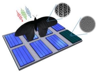
Sunlight reflected by solar cells is lost as unused energy. The wings of the butterfly Pachliopta aristolochiae are drilled by nanostructures (nanoholes) that help absorbing light over a wide spectrum far better than smooth surfaces. Researchers of Karlsruhe Institute of Technology (KIT) have now succeeded in transferring these nanostructures to solar cells and, thus, enhancing their light absorption rate by up to 200%.
Image caption: Nanostructures of the wing of Pachliopta aristolochiae can be transferred to solar cells and enhance their absorption rates by up to 200%. (Graphics: Radwanul H. Siddique, KIT/Caltech)
“The butterfly studied by us is very dark black. This signifies that it perfectly absorbs sunlight for optimum heat management. Even more fascinating than its appearance are the mechanisms that help reaching the high absorption. The optimization potential when transferring these structures to photovoltaics (PV) systems was found to be much higher than expected,” says Dr. Hendrik Hölscher of KIT’s Institute of Microstructure Technology (IMT).
The scientists of the team of Hendrik Hölscher and Radwanul H. Siddique (formerly KIT, now Caltech) reproduced the butterfly’s nanostructures in the silicon absorbing layer of a thin-film solar cell. Subsequent analysis of light absorption yielded promising results: Compared to a smooth surface, the absorption rate of perpendicular incident light increases by 97% and rises continuously until it reaches 207% at an angle of incidence of 50 degrees. “This is particularly interesting under European conditions. Frequently, we have diffuse light that hardly falls on solar cells at a vertical angle,” Hendrik Hölscher says.
However, this does not automatically imply that efficiency of the complete PV system is enhanced by the same factor, says Guillaume Gomard of IMT. “Also other components play a role. Hence, the 200% are to be considered a theoretical limit for efficiency enhancement.”
Prior to transferring the nanostructures to solar cells, the researchers determined the diameter and arrangement of the nanoholes on the wing of the butterfly by means of scanning electron microscopy. Then, they analyzed the rates of light absorption for various hole patterns in a computer simulation. They found that disordered holes of varying diameters, such as those found in the black butterfly, produced most stable absorption rates over the complete spectrum at variable angles of incidence, with respect to periodically arranged monosized nanoholes. Hence, the researchers introduced disorderly positioned holes in a thin-film PV absorber, with diameters varying from 133 to 343 nanometers.
The scientists demonstrated that light yield can be enhanced considerably by removing material. In the project, they worked with hydrogenated amorphous silicon. According to the researchers, however, any type of thin-film PV technology can be improved with such nanostructures, also on the industrial scale.
Background information:
Thin-film PV modules represent an economically attractive alternative to conventional crystalline silicon solar cells, as the light-absorbing layer is thinner by a factor of up to 1000 and, hence, material consumption is reduced. Still, absorption rates of thin layers are below those of crystalline silicon cells. Hence, they are used in systems needing little power, such as pocket calculators or watches. Enhanced absorption would make thin-film cells much more attractive for larger applications, such as photovoltaics systems on roofs.
Being ”The Research University in the Helmholtz Association“, KIT creates and imparts knowledge for the society and the environment. It is the objective to make significant contributions to the global challenges in the fields of energy, mobility and information. For this, about 9,300 employees cooperate in a broad range of disciplines in natural sciences, engineering sciences, economics, and the humanities and social sciences. KIT prepares its 26,000 students for responsible tasks in society, industry, and science by offering research-based study programs. Innovation efforts at KIT build a bridge between important scientific findings and their application for the benefit of society, economic prosperity, and the preservation of our natural basis of life.
Share on:


Suggested Items
Duality AI Contracts with NASA JPL for Phase II of DARPA RACER Program
09/13/2024 | BUSINESS WIREDuality AI, the company behind Falcon, a digital twin simulation platform, today announced an agreement with NASA’s Jet Propulsion Laboratory (NASA JPL) in Pasadena to continue its work on Defense Advanced Research Projects Agency’s (DARPA’s) Robotic Autonomy in Complex Environments with Resiliency program (RACER).
Electronic Design Automation Market Valuation is Poised to Reach $35.3 Billion By 2032
08/08/2024 | Globe NewswireThe global electronic design automation market is projected to hit the market valuation of US$35.3 billion by 2032 from $15.8 billion in 2023 and at a CAGR of 9.75% during the forecast period 2024–2032.
CACI Awarded $319 Million Task Order to Provide Intelligence Systems Expertise to the U.S. Army
08/05/2024 | CAC, Inc.CACI International Inc announced that it has been awarded a five-year task order valued at up to $319 million to provide intelligence systems expertise to the U.S. Army, Communications-Electronics Command (CECOM), Software Engineering Center (SEC), Electronic Warfare and Sensors Directorate (IEWSD), Army Reprogramming Analysis Team-Program Office (ARAT-PO).
Ansys 2024 R2 Delivers Multiphysics Innovation Across Industries and Engineering Domains
07/29/2024 | ANSYSAnsys 2024 R2 redefines the boundaries of product design by enabling customers to move beyond the limits of single-physics simulation to gain multidimensional insight into the performance of today’s complex products. R2 enhancements focused on accelerating run times, scaling capacity, enabling digital transformation, and providing hardware flexibility are making Ansys multiphysics simulations more accessible and powerful than ever before.
Altair to Showcase Cutting-Edge AI-Powered Engineering at Farnborough International Airshow 2024
07/19/2024 | AltairAltair, a global leader in computational intelligence, will showcase its latest innovations in engineering simulation, artificial intelligence (AI), and high-performance computing (HPC) at the Farnborough International Airshow 2024.