


 Beyond the Board: What Companies Need to Know Before Entering the MilAero PCB Market
 Defense Speak Interpreted: If CHIPS Cuts Back, What Happens to Electronics Packaging Funds?
 American Made Advocacy: Where’s the Budget for a Modern Military Run on Microelectronics?


Developing 'ABCs' for Exploiting New Phenomena in Light-Matter Interactions
November 16, 2017 | DARPAEstimated reading time: 3 minutes
A unique class of engineered light-manipulating materials, known as metamaterials or structured materials, makes use of patterns of strongly interacting wavelength or sub-wavelength-sized elements. Because of these intricate internal and surface structures, new properties have emerged, some exhibiting behavior that has resulted in rewriting long-understood “laws” for how light and other electromagnetic (EM) waves interact with materials.
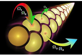
Image Caption: DARPA's Nascent Light-Matter Interactions (NLM) program aims to develop theory-anchored models that could yield new structures for materials with never-before-seen electromagnetic properties. This artist's concept depicts an example of how an engineered material might be able to convert, generate, or harvest electromagnetic fields exploiting interactions that could have far-reaching effects in areas such as sensing, thermal control, frequency conversion, and dynamics.
These materials have been opening up new options for controlling EM waves in many technological arenas, among them imaging, thermal control, and frequency conversion. Specific applications include night-vision, heat reflection and management in aircraft engines, and temperature regulation of electronics on satellites in the hot-and-cold extremes of space.
Although researchers have been taking steps toward putting these materials to practical use, they remain puzzled about the optimal structure designs for desired matter-light interactions. They have yet to model the materials in ways that enable predictions about how specific structured materials will behave under different conditions, such as increased illumination intensities. To fill in these knowledge gaps, DARPA today announced the Nascent Light-Matter Interactions (NLM) program, which seeks to finally develop theory-anchored models that can expand the state of the art in already-observed phenomena while pointing to never-before-realized and new functionality.
“Recent advances in our understanding of light-matter interactions have revealed nascent concepts that could yield new materials with properties way beyond anything we have now,” said Mike Fiddy, DARPA program manager. “Through NLM we aim to identify building blocks to better understand the physics of 2-D and 3-D structured materials, which can then lead to a systematic design approach for controlling electromagnetic waves through these materials. The end goal is to equip designers with rigorous predictive models and design tools to answer the currently elusive question: ‘If I want a material with X property, how do I build it?’”
For example, can we open new pathways for designing materials that provide more efficiency in up-conversion or down conversion of frequencies, which could benefit military capabilities such as night vision? “At the moment, the state-of-the-art of these complicated structures is you pump them with one frequency and they’ll emit maybe 10 percent at another frequency, but they require lots of power in the process,” he said. “Can we develop design tools to create materials with 80, 90, or 100 percent efficiency in converting infrared light into visible light that require very little or no power?”
As Fiddy sees it, lessons learned in the NLM program also might help engineers design better materials, for example, that automatically block the frequency of a laser if it’s shined directly into the eye. Another example is managing extremely hot temperatures, such as those found in turbine aircraft engines. New engineered materials could help precisely manage temperatures in critical hot parts of the engine, which in turn could lead to more efficiency, thus reducing fuel and maintenance costs.
“Similarly, on satellites, as they orient toward the sun they can get ‘cooked’ and when they are out of the sun they are very cold,” Fiddy said. “Those big temperature extremes have to be controlled somehow in the satellite’s design. But if there were more efficient ways of radiating away the sun’s heat using structured materials, that would be very valuable. A general approach to solving this problem could be beneficial for keeping computer chips cool while at the same time opening up new ways to harvest electromagnetic energy.”
It could take years to realize such possibilities, Fiddy noted, but he hopes the NLM program will deliver new levels of understanding and modeling tools that could hasten that day. As such, he added, this new program should benefit existing programs, such as EXTREME, which focuses on specific uses for engineered materials.
The NLM program will unfold in three phases. The first will challenge performers to develop a model and show that it can predict new phenomena and serve as a design tool. The second phase will push researchers to test the models’ actual utility for identifying new materials useful for specific applications. The goal for Phase 3 is to identify specific challenge problems and tie selected performers and their respective focus and applications to the operational needs of DoD stakeholders.
Share on:


Testimonial
"Advertising in PCB007 Magazine has been a great way to showcase our bare board testers to the right audience. The I-Connect007 team makes the process smooth and professional. We’re proud to be featured in such a trusted publication."
Klaus Koziol - atgSuggested Items
Staying on Top of Signal Integrity Challenges
09/16/2025 | Andy Shaughnessy, Design007 MagazineOver the years, Kris Moyer has taught a variety of advanced PCB design classes, both online IPC courses and in-person classes at California State University-Sacramento, where he earned his degrees in electrical engineering. Much of his advanced curriculum focuses on signal integrity, so we asked Kris to discuss the trends he’s seeing in signal integrity today, the SI challenges facing PCB designers, and his go-to techniques for controlling or completely eliminating SI problems.
ASM Technologies Limited signs MoU with the Guidance, Government of Tamilnadu to Expand Design-Led Manufacturing capabilities for ESDM
09/15/2025 | ASM TechnologiesASM Technologies Limited, a pioneer in Design- Led Manufacturing in the semiconductor and automotive industries, announced signing of Memorandum of Understanding (MoU) with the Guidance, Government of Tamilnadu whereby it will invest Rs. 250 crores in the state to expand its ESDM related Design-Led Manufacturing and precision engineering capacity. ASM Technologies will acquire 5 acres of land from the Government of Tamilnadu to set up a state-of-the-art design facility in Tamil Nadu's growing technology manufacturing ecosystem, providing a strong strategic advantage and long-term benefits for ASM.
Variosystems Strengthens North American Presence with Southlake Relaunch 2025
09/15/2025 | VariosystemsVariosystems celebrated the relaunch of its U.S. facility in Southlake, Texas. After months of redesign and reorganization, the opening marked more than just the return to a modernized production site—it was a moment to reconnect with our teams, partners, and the local community.
Deca, Silicon Storage Technology Announce Strategic Collaboration to Enable NVM Chiplet Solutions
09/11/2025 | Microchip Technology Inc.As traditional monolithic chip designs grow in complexity and increase in cost, the interest and adoption of chiplet technology in the semiconductor industry also increases.
I-Connect007 Launches New Podcast Series on Ultra High Density Interconnect (UHDI)
09/10/2025 | I-Connect007I-Connect007 is excited to announce the debut of its latest podcast series, which shines a spotlight on one of the most important emerging innovations in electronics manufacturing: Ultra-High-Density Interconnect (UHDI). The series kicks off with Episode One, “Ultra HDI: What does it mean to people? Why would they want it?” Host Nolan Johnson is joined by guest expert John Johnson, Director of Quality and Advanced Technology at American Standard Circuits (ASC).