


 The Right Approach: The Pros and Cons of PCB Vertical Integration
 American Made Advocacy: PCBAA’s Fifth Annual Meeting—Growing Membership and Valuable Relationships
 It's Only Common Sense: Why the Best Years of Electronics Are Still Ahead of Us


In the early history of electronic devices, germanium, a more efficient elemental semiconductor than silicon, was the material of choice. Ultimately, the high cost of developing germanium crystals eclipsed its efficiency, and silicon captured the field. But new research establishing an economical method for growing crystalline thin-film germanium – using a process known as van der Waals epitaxy — challenges that supremacy.
“This is the first time strain-free van der Waals epitaxy of an elemental semiconductor has been demonstrated,” said Aaron Littlejohn, a doctoral candidate in the laboratory of Gwo-Ching Wang, professor of physics, applied physics, and astronomy at Rensselaer Polytechnic Institute. “Our research found a narrow window, a very specific set of conditions that work.”
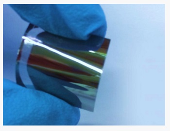
Interestingly, the technique produces flexible germanium that which can be removed from the substrate.
“Our germanium film could be used as a thin-film nanomembrane, which could be integrated into electronic devices more easily than nanocrystals or nanowires,” said Littlejohn, who is first author on the research. “It could also serve as the substrate for the subsequent deposition of additional materials for flexible transistors and solar cells, or even wearable optoelectronics.”
To efficiently conduct electrical charge, the atoms in semiconducting materials must be consistently arranged in a precise crystal lattice. To produce that consistent lattice, semiconductor fabricators employ a phenomenon known as epitaxy, and deposit a thin film layer of the desired semiconducting material on an expendable crystalline substrate. As they are deposited, the atoms of the semiconducting material align with the crystal pattern of the substrate. If the film and the substrate materials have the same pattern, the perfectly matched layers produce strong chemical bonds for optimal electrical charge carrier mobility.
If the atomic spacings, or periodicities, of the semiconductor and the substrate aren’t a good match, conventional epitaxy creates a material compromised by strain and defects, which decreases carrier mobility. There are few good matches for germanium, and those that exist, like gallium arsenide, are expensive, driving up the cost of manufacturing.
To solve the problem, the researchers grew germanium film on a substrate of muscovite mica, a material whose atoms assemble in layers, with no chemical bonds between layers. The surface of a layer of mica is free of dangling bonds, ensuring that germanium, as it is deposited, will not chemically bond with or adhere to the periodicity of the mica.
Instead, the arrangement of germanium atoms is guided by van der Waals forces, weakly attractive interactions between neutral atoms, based on the probabilistic nature of electrons. This allows the germanium to grow in a relaxed film, despite the dramatically different crystal structures of the two materials (a 23 percent difference in atomic spacing).
The researchers grew germanium films about 80 nanometers thick on muscovite mica substrates 75 millimeters long, 25 millimeters wide, and .26 mm thick. By varying the substrate temperature during deposition and annealing in the range of 300-500 degrees Celsius, the researchers found that the crystal lattice stabilizes at about 425 degrees Celsius.
“Previous research implies that elemental semiconductors cannot be epitaxially grown on mica using van der Waals forces at any elevated temperature, but we have now shown otherwise,” Littlejohn said. “With the success of our germanium film grown on mica at a practical temperature, we anticipate that other nonlayered elemental or alloyed materials can be grown on mica via van der Waals epitaxy.”
The research fulfills The New Polytechnic, an emerging paradigm for higher education which recognizes that global challenges and opportunities are so great they cannot be adequately addressed by even the most talented person working alone. Rensselaer serves as a crossroads for collaboration — working with partners across disciplines, sectors, and geographic regions — to address complex global challenges, using the most advanced tools and technologies, many of which are developed at Rensselaer. Research at Rensselaer addresses some of the world’s most pressing technological challenges — from energy security and sustainable development to biotechnology and human health. The New Polytechnic is transformative in the global impact of research, in its innovative pedagogy, and in the lives of students at Rensselaer.
About Rensselaer Polytechnic Institute
Rensselaer Polytechnic Institute, founded in 1824, is America’s first technological research university. For nearly 200 years, Rensselaer has been defining the scientific and technological advances of our world. Rensselaer faculty and alumni represent 85 members of the National Academy of Engineering, 17 members of the National Academy of Sciences, 25 members of the American Academy of Arts and Sciences, 8 members of the National Academy of Medicine, 8 members of the National Academy of Inventors, and 5 members of the National Inventors Hall of Fame, as well as 6 National Medal of Technology winners, 5 National Medal of Science winners, and a Nobel Prize winner in Physics. With 7,000 students and nearly 100,000 living alumni, Rensselaer is addressing the global challenges facing the 21st century—to change lives, to advance society, and to change the world.


