


 Trouble in Your Tank: Implementing Direct Metallization in Advanced Substrate Packaging
 It’s Only Common Sense: Storytelling That Sells—Stop Pitching, Start Painting Pictures
 The Right Approach: Get Ready for ISO 9001 Version 6


Optoelectronics Origami: an Easy-To-Make, Double-Duty Curved Image Sensor
November 27, 2017 | University of Wisconsin-MadisonEstimated reading time: 2 minutes
Cellphone users rely on their phone cameras to capture virtually every aspect of their lives. Far too often, however, they end up with photos that are a sub-par reproduction of reality.
While operator error sometimes comes into play, the camera’s digital image sensor is the most likely culprit. A flat, silicon surface, it just can’t process images captured by a curved camera lens as well as the similarly curved image sensor — otherwise known as the retina — in a human eye.
In an advance that could lead to cameras with features such as infinite depth of field, wider view angle, low aberrations, and vastly increased pixel density, flexible optoelectronics pioneer Zhenqiang (Jack) Ma has devised a method for making curved digital image sensors in shapes that mimic the convex features of an insect’s compound eye and a mammal’s concave “pinhole” eye.
Along with his students and collaborators, Ma, the Lynn H. Matthias and Vilas Distinguished Achievement Professor of Electrical and Computer Engineering at the University of Wisconsin–Madison, described the technique in a study published today (Nov. 24, 2017) in the journal Nature Communications.
Curved image sensors do exist. Yet even though they outperform their flat counterparts, they haven’t made it into the mainstream — in part, because of the challenges inherent in a manufacturing method that involves pressing a flat, rigid piece of silicon into a hemispherical shape without wrinkling or breaking it or otherwise degrading its quality.
Ma’s technique was inspired by traditional Japanese origami, the art of paper folding.
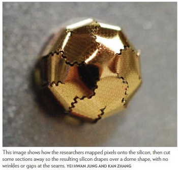
To create the curved photodetector, Ma and his students formed pixels by mapping repeating geometric shapes — somewhat like a soccer ball — onto a thin, flat flexible sheet of silicon called a nanomembrane, which sits on a flexible substrate. Then, they used a laser to cut away some of those pixels so the remaining silicon formed perfect, gapless seams when they placed it atop a dome shape (for a convex detector) or into a bowl shape (for a concave detector).
“We can first divide it into a hexagon and pentagon structure, and each of those can be further divided,” says Ma. “You can forever divide them, in theory, so that means the pixels can be really, really dense, and there are no empty areas. This is really scalable, and we can bend it into whatever shape we want.”
Pixel density is a boon for photographers, as a camera’s ability to take high-resolution photos is determined, in megapixels, by the amount of information its sensor can capture.
The researchers’ current prototype is approximately 7 millimeters — roughly a quarter-inch — in diameter. That’s still a bit bulky for your cellphone, but Ma says he can make the sensor even smaller.
“This membrane is a very big advance in imaging,” he says.
Share on:


Testimonial
"Advertising in PCB007 Magazine has been a great way to showcase our bare board testers to the right audience. The I-Connect007 team makes the process smooth and professional. We’re proud to be featured in such a trusted publication."
Klaus Koziol - atgSuggested Items
Printed Electronics Market Size to Top $83.77 Billion by 2034 Driven by IoT Adoption and Flexible Device Demand
09/11/2025 | Globe NewswireThe printed electronics market size has been calculated at U$19,920 million in 2025 and is expected to grow from $23,58 million in 2026 to approximately $83,770 million by 2034.
Fresh PCB Concepts: Designing for Success at the Rigid-flex Transition Area
08/28/2025 | Team NCAB -- Column: Fresh PCB ConceptsRigid-flex PCBs come in all shapes and sizes. Manufacturers typically use fire-retardant, grade 4 (FR-4) materials in the rigid section and flexible polyimide materials in the flex region. Because of the small size, some rigid-flex PCBs, like those for hearing aid devices, are among the most challenging to manufacture. However, regardless of its size, we should not neglect the transition area between the rigid and flexible material.
Global Flexible PCB Output Expected to Surpass $20 Billion by 2025, with AI Glasses Emerging as a New Growth Driver
08/25/2025 | TPCAThe Taiwan Printed Circuit Association (TPCA) and the Industrial Technology Research Institute (ITRI) released the "2025 Global Flexible PCB Industry Outlook" in August.
Nano Silver Inks Market Forecast Report 2025-2030
08/20/2025 | Globe NewswireThe Nano Silver Inks Market is expected to grow from USD 427.415 million in 2025 to USD 836.160 million in 2030, at a CAGR of 14.36%.
Flexible Circuit Technologies to Host Free Flex Heater Webinar
08/18/2025 | Flexible Circuit TechnologiesGlobal Supplier of flexible circuits, flex design services, and assembly/box-build services, Flexible Circuit Technology will host their latest webinar, "Thermal Precision Meets Flexibility: The Technology Behind Heater Circuits" on Tuesday, August 26th, 2025 at 11 AM EDT.