


 Trouble in Your Tank: Implementing Direct Metallization in Advanced Substrate Packaging
 It’s Only Common Sense: Storytelling That Sells—Stop Pitching, Start Painting Pictures
 The Right Approach: Get Ready for ISO 9001 Version 6


Fast Flowing Heat in Graphene Heterostructures
November 30, 2017 | ICFOEstimated reading time: 1 minute
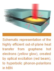
Nanoscale heat flow plays a crucial role in many modern electronic and optoelectronic applications, such as thermal management, photodetection, thermoelectrics and data communication. Two-dimensional layered materials are beginning to confirm their groundbreaking role in many of these applications. Perhaps even more promising are so-called van der Waals heterostructures, consisting of different layered two-dimensional materials stacked one on top of the other. These stacks can consist of materials with dramatically different physical properties, while the interfaces between them are ultraclean and atomically sharp.
Scientists from the European Graphene Flagship, led by ICFO researchers, have recently succeeded in observing and following, in real-time, the way in which heat transport occurs in van der Waals stacks, which consist of graphene encapsulated by the dielectric two-dimensional material hexagonal BN (hBN).
In a study, recently published in Nature Nanotechnology entitled “Out-of-plane heat transfer in van der Waals stacks through electron–hyperbolic phonon coupling” , ICFO researchers Klaas-Jan Tielrooij, Niels C. H. Hesp, Mark B. Lundeberg, Mathieu Massicotte, Peter Schmidt, and Diana Davydovskaya, led by ICREA Prof at ICFO Frank Koppens, in collaboration with researchers from The Netherlands, Italy, Germany, and United Kingdom, have identified a highly surprisingly effect: rather than staying within the graphene sheet, the heat actually flows to the surrounding hBN sheets. This out-of-plane heat transfer process occurs on an ultrafast timescale of picoseconds (one millionth of a millionth of a second), and is therefore dominant over competing (in-plane) heat transfer processes.
The heat transfer process occurs through hot graphene electrons (experimentally generated by incident light) that couple to hyperbolic phonon-polaritons in the hBN sheets. These phonon-polaritons propagate within the hBN as light does in an optical fiber, but in this case for infrared wavelengths and at the nanometer scale. It turns out that these exotic hyperbolic modes are very efficient at carrying heat away.
The results of this work will definitely have far-reaching implications for many applications based on hBN-encapsulated graphene, sometimes referred to as the next generation graphene platform, owing to its superior electrical properties. In particular, it will provide direction to optoelectronic device design, where these heat flow processes can be thoroughly exploited.
Share on:


Testimonial
"Advertising in PCB007 Magazine has been a great way to showcase our bare board testers to the right audience. The I-Connect007 team makes the process smooth and professional. We’re proud to be featured in such a trusted publication."
Klaus Koziol - atgSuggested Items
September 2025 PCB007 Magazine: The Future of Advanced Materials
09/16/2025 | I-Connect007 Editorial TeamMoore’s Law is no more, and the advanced material solutions being developed to grapple with this reality are surprising, stunning, and perhaps a bit daunting. Buckle up for a dive into advanced materials and a glimpse into the next chapters of electronics manufacturing.
I-Connect007 Launches Advanced Electronics Packaging Digest
09/15/2025 | I-Connect007I-Connect007 is pleased to announce the launch of Advanced Electronics Packaging Digest (AEPD), a new monthly digital newsletter dedicated to one of the most critical and rapidly evolving areas of electronics manufacturing: advanced packaging at the interconnect level.
Panasonic Industry will Double the Production Capacity of MEGTRON Multi-layer Circuit Board Materials Over the Next Five Years
09/15/2025 | Panasonic Industry Co., Ltd.Panasonic Industry Co., Ltd., a Panasonic Group company, announced plans for a major expansion of its global production capacity for MEGTRON multi-layer circuit board materials today. The company plans to double its production over the next five years to meet growing demand in the AI server and ICT infrastructure markets.
Trouble in Your Tank: Implementing Direct Metallization in Advanced Substrate Packaging
09/15/2025 | Michael Carano -- Column: Trouble in Your TankDirect metallization systems based on conductive graphite are gaining popularity throughout the world. The environmental and productivity gains achievable with this process are outstanding. Direct metallization reduces the costs of compliance, waste treatment, and legal issues related to chemical exposure. A graphite-based direct plate system has been devised to address these needs.
Fresh PCB Concepts: Designing for Success at the Rigid-flex Transition Area
08/28/2025 | Team NCAB -- Column: Fresh PCB ConceptsRigid-flex PCBs come in all shapes and sizes. Manufacturers typically use fire-retardant, grade 4 (FR-4) materials in the rigid section and flexible polyimide materials in the flex region. Because of the small size, some rigid-flex PCBs, like those for hearing aid devices, are among the most challenging to manufacture. However, regardless of its size, we should not neglect the transition area between the rigid and flexible material.