


 Trouble in Your Tank: Implementing Direct Metallization in Advanced Substrate Packaging
 It’s Only Common Sense: Storytelling That Sells—Stop Pitching, Start Painting Pictures
 The Right Approach: Get Ready for ISO 9001 Version 6


Quantum Waltz of Electrons Hints at the Next Generation of Chips
December 6, 2017 | EPFLEstimated reading time: 2 minutes
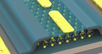
EPFL researchers have successfully measured some of the quantum properties of electrons in two-dimensional semiconductors. This work in the field of spintronics could one day lead to chips that are not only smaller but that also generate less heat.
A group of spintronics researchers at EPFL is using new materials to reveal more of the many capabilities of electrons. The field of spintronics seeks to tap the quantum properties of “spin,” the term often used to describe one of the fundamental properties of elementary particles – in this case, electrons. This is among the most cutting-edge areas of research in electronics today.
Researchers working in the Laboratory of Nanoscale Electronics and Structures (LANES), which is run by Professor Andras Kis, were able to quantify these quantum properties for a category of two-dimensional semiconductors called transition metal dichalcogenides, or TMDCs. Their research projects, which were published recently in ACS Nano and today in Nature Communications, confirm that materials like graphene (C), molybdenite (MoS2) and tungsten diselenide (WSe2) offer, either alone or by combining some of their characteristics, new perspectives for the field of electronics – perspectives that could ultimately lead to smaller chips that generate less heat.
“With the methods we’ve recently developed, we’ve shown that it is possible to access the spin in these TMDC materials, quantify it and use it to introduce new functionalities,” says Kis.
This all takes place at an extremely small scale. In order to access these quantum properties, the researchers must work with high quality materials. “If we want to examine certain characteristics of electrons, including their energy, we need to be able to watch them move over relatively long distances without there being too much dispersion or disruption,” explains Kis.
In the form of waves
The researchers’ method allows them to obtain samples of sufficient quality both to observe how electrons move around in the form of waves and to quantify their energy.
But the LANES team was also able to access another quantum property. Spins of electrons and holes in this type of a 2D semiconductor can be in one of two states, which are conventionally described as being oriented upward – spin up – or downward – spin down. Their energy will be slightly different in each of these two states. That’s called spin splitting, and the EPFL researchers have measured it for the first time for electrons in TMDC materials.
In the second publication, the researchers wrote about how they used the spin splitting in a TMDC in order to introduce polarized spin currents in graphene without using a magnetic field.
These discoveries are a step forward for the emerging field of spintronics and make it increasingly likely that a different property of charge carriers – i.e. spin, in addition to the electrical charge – will play a role in tomorrow’s electronic devices.
Share on:


Testimonial
"Advertising in PCB007 Magazine has been a great way to showcase our bare board testers to the right audience. The I-Connect007 team makes the process smooth and professional. We’re proud to be featured in such a trusted publication."
Klaus Koziol - atgSuggested Items
September 2025 PCB007 Magazine: The Future of Advanced Materials
09/16/2025 | I-Connect007 Editorial TeamMoore’s Law is no more, and the advanced material solutions being developed to grapple with this reality are surprising, stunning, and perhaps a bit daunting. Buckle up for a dive into advanced materials and a glimpse into the next chapters of electronics manufacturing.
I-Connect007 Launches Advanced Electronics Packaging Digest
09/15/2025 | I-Connect007I-Connect007 is pleased to announce the launch of Advanced Electronics Packaging Digest (AEPD), a new monthly digital newsletter dedicated to one of the most critical and rapidly evolving areas of electronics manufacturing: advanced packaging at the interconnect level.
Panasonic Industry will Double the Production Capacity of MEGTRON Multi-layer Circuit Board Materials Over the Next Five Years
09/15/2025 | Panasonic Industry Co., Ltd.Panasonic Industry Co., Ltd., a Panasonic Group company, announced plans for a major expansion of its global production capacity for MEGTRON multi-layer circuit board materials today. The company plans to double its production over the next five years to meet growing demand in the AI server and ICT infrastructure markets.
Trouble in Your Tank: Implementing Direct Metallization in Advanced Substrate Packaging
09/15/2025 | Michael Carano -- Column: Trouble in Your TankDirect metallization systems based on conductive graphite are gaining popularity throughout the world. The environmental and productivity gains achievable with this process are outstanding. Direct metallization reduces the costs of compliance, waste treatment, and legal issues related to chemical exposure. A graphite-based direct plate system has been devised to address these needs.
Fresh PCB Concepts: Designing for Success at the Rigid-flex Transition Area
08/28/2025 | Team NCAB -- Column: Fresh PCB ConceptsRigid-flex PCBs come in all shapes and sizes. Manufacturers typically use fire-retardant, grade 4 (FR-4) materials in the rigid section and flexible polyimide materials in the flex region. Because of the small size, some rigid-flex PCBs, like those for hearing aid devices, are among the most challenging to manufacture. However, regardless of its size, we should not neglect the transition area between the rigid and flexible material.