


 Trouble in Your Tank: Implementing Direct Metallization in Advanced Substrate Packaging
 It’s Only Common Sense: Storytelling That Sells—Stop Pitching, Start Painting Pictures
 The Right Approach: Get Ready for ISO 9001 Version 6


Tiny Structures Could Be Next-Generation Solution for Smaller Electronic Devices
December 8, 2017 | UCLA NewsroomEstimated reading time: 2 minutes
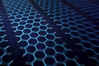
Silicon — the shiny, brittle metal commonly used to make semiconductors — is an essential ingredient of modern-day electronics. But as electronic devices have become smaller and smaller, creating tiny silicon components that fit inside them has become more challenging and more expensive.
Now, UCLA chemists have developed a new method to produce nanoribbons of graphene, next-generation structures that many scientists believe will one day power electronic devices.
The nanoribbons are extremely narrow strips of graphene, the width of just a few carbon atoms. They’re useful because they possess a bandgap, which means that electrons must be “pushed” to flow through them to create electrical current, said Yves Rubin, a professor of chemistry in the UCLA College and the lead author of the research.
“A material that has no bandgap lets electrons flow through unhindered and cannot be used to build logic circuits,” he said.
Rubin and his research team constructed graphene nanoribbons molecule by molecule using a simple reaction based on ultraviolet light and exposure to 600-degree heat.
“Nobody else has been able to do that, but it will be important if one wants to build these molecules on an industrial scale,” said Rubin, who also is a member of the California NanoSystems Institute at UCLA.
The process improves upon other existing methods for creating graphene nanoribbons, one of which involves snipping open tubes of graphene known as carbon nanotubes. That particular approach is imprecise and produces ribbons of inconsistent sizes — a problem because the value of a nanoribbon’s bandgap depends on its width, Rubin said.
To create the nanoribbons, the scientists started by growing crystals of four different colorless molecules. The crystals locked the molecules into the perfect orientation to react, and the team then used light to stitch the molecules into polymers, which are large structures made of repeating units of carbon and hydrogen atoms.
The scientists then placed the shiny, deep blue polymers in an oven containing only argon gas and heated them to 600 degrees Celsius. The heat provided the necessary boost of energy for the polymers to form the final bonds that gave the nanoribbons their final shape: hexagonal rings composed of carbon atoms, and hydrogen atoms along the edges of the ribbons.
“We’re essentially charring the polymers, but we’re doing it in a controlled way,” Rubin said.
The process, which took about an hour, yielded graphene nanoribbons just eight carbon atoms wide but thousands of atoms long. The scientists verified the molecular structure of the nanoribbons, which were deep black in color and lustrous, by shining light of different wavelengths at them.
“We looked at what wavelengths of light were absorbed,” Rubin said. “This reveals signatures of the structure and composition of the ribbons.”
The researchers have filed a patent application for the process.
Rubin said the team now is studying how to better manipulate the nanoribbons — a challenge because they tend to stick together.
“Right now, they are bundles of fibers,” Rubin said. “The next step will be able to handle each nanoribbon one by one.”
The study’s co-authors include Richard Kaner, a UCLA distinguished professor of chemistry and biochemistry, and of materials science and engineering; Kendall Houk, UCLA’s Saul Winstein Professor of Organic Chemistry; Robert Jordan, a former UCLA graduate student; UCLA graduate students Yolanda Li, Cheng-Wei Lin, Janice Lin and Kris Marsh; and Ryan McCurdy, a UCLA undergraduate student.
Share on:


Testimonial
"Advertising in PCB007 Magazine has been a great way to showcase our bare board testers to the right audience. The I-Connect007 team makes the process smooth and professional. We’re proud to be featured in such a trusted publication."
Klaus Koziol - atgSuggested Items
Rules of Thumb: Design007 Magazine, November 2024
11/11/2024 | I-Connect007 Editorial TeamRules of thumb are everywhere, but there may be hundreds of rules of thumb for PCB design. They’re built on design formulas, fabricators’ limitations, and tribal knowledge. And unfortunately, some longtime rules of thumb should be avoided at all costs. How do we separate the wheat from the chaff, so to speak?
Connect the Dots: Best Practices for Prototyping
09/21/2023 | Matt Stevenson -- Column: Connect the DotsPCB prototyping is a critical juncture during an electronic device’s journey from concept to reality. Regardless of a project’s complexity, the process of transforming a design into a working board is often enlightening in terms of how a design can be improved before a PCB is ready for full production.
The Drive Toward UHDI and Substrates
09/20/2023 | I-Connect007 Editorial TeamPanasonic’s Darren Hitchcock spoke with the I-Connect007 Editorial Team on the complexities of moving toward ultra HDI manufacturing. As we learn in this conversation, the number of shifting constraints relative to traditional PCB fabrication is quite large and can sometimes conflict with each other.
Asia/Pacific AI Spending Surge to Reach a Projected $78 Billion by 2027
09/19/2023 | IDCAsia/Pacific spending on Artificial Intelligence (AI) ), including software, services, and hardware for AI-centric systems will grow to $78.4 billion in 2027, according to International Data Corporation's latest Worldwide Artificial Intelligence Spending Guide.
Intel to Sell Minority Stake in IMS Nanofabrication Business to TSMC
09/13/2023 | IntelIntel Corporation announced that it has agreed to sell an approximately 10% stake in the IMS Nanofabrication business to TSMC. TSMC’s investment values IMS at approximately $4.3 billion, consistent with the valuation of the recent stake sale to Bain Capital Special Situations.