


 Trouble in Your Tank: Implementing Direct Metallization in Advanced Substrate Packaging
 It’s Only Common Sense: Storytelling That Sells—Stop Pitching, Start Painting Pictures
 The Right Approach: Get Ready for ISO 9001 Version 6


Three Kinds of Information from a Single X-Ray Measurement
December 11, 2017 | Friedrich-Schiller-Universitaet JenaEstimated reading time: 3 minutes
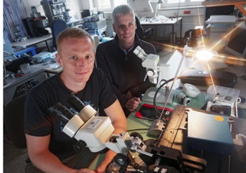
Whatever the size of mobile phones or computers are, the way in which such electronic devices operate relies on the interaction between various materials. For this reason, engineers as well as researchers need to know exactly how specific chemical elements inside a computer chip or a transistor diode behave, and what happens when these elements bond. Physicists of Friedrich Schiller University Jena, Germany, have now developed an innovative method that enables them to obtain several different types of information simultaneously from the interior of a nanoscale building block - and this while it is in the active state. The researchers from Jena and their partners have reported their findings in the current issue of the specialist journal "Science Advances".
"Using our method, we can obtain information at one and the same time about the elements' composition, that is to say the fraction between the elements; about their oxidation grade, which means their valence state or the nature of the bond; and finally about internal electrical fields that have thus been created," explains Prof. Dr Carsten Ronning of the University of Jena. "These are all elementary indicators for the component's function," adds Ronning, who heads the project. However, in the procedure developed by the physicists from Jena, together with colleagues from Grenoble, Madrid and Vienna, the components to be investigated do not have to be elaborately prepared or possibly even destroyed. "In principle, we can X-ray the diodes of a mobile phone while it is switched on, without damaging it," says Ronning.
X-ray beam from the particle accelerator
A decisive feature of the research approach is a very finely focussed X-ray beam, with which the Jena physicists initially X-rayed a device specially made for their experiments. "We introduced arsenic and gallium atoms into a silicon wire around 200 nanometres thick. When heated, these atoms agglomerate at one point, that is to say they mass together, which produces a functional component," explains Prof. Ronning. "We then ran a 50-nanometre-wide X-ray beam along the wire, thus irradiating it bit by bit." The researchers established that - such as in a solar cell - this arrangement mixture of materials converted the X-rays into electric current, which flowed only in one direction, as in a diode. In this way, the researchers made the internal electrical fields visible that are essential for the function of the component. In addition, the component emitted light. "The X-rays excite the atoms in the building block, which emit a characteristic radiation," explains Dr Andreas Johannes, who conducted the experiments. "In this way we obtain a spectrum, which gives us valuable information about the individual elements present and their relative ratios." If the energy of the X-rays is altered, so called X-ray absorption spectra are produced that enable researchers to make assertions regarding the oxidation grade of the elements - and by extension regarding the bonds themselves.
Obtain all these types of information through one measurement
"Now, it is possible to obtain all these types of information through one measurement by using our method," says Andreas Johannes. Although comparable results are possible using electron microscopy, in these cases the devices have to be specially prepared and possibly destroyed, as the penetration depth of the electron beam is substantially more limited. Moreover, such measurements can only take place in a vacuum, whereas the X-ray method is virtually independent of any specific environment.
Up to now, such narrow X-ray beams can only be generated by particle accelerators, which is why the Jena University physicists have been working together closely with the European Synchrotron Radiation Facility (ESRF) in Grenoble, France, to develop the new measuring method. These facilities are available to both, scientific researchers and industry, in order to X-ray existing components with greater precision and, above all, to try out new combinations of materials in order to create better performing components. "For example, our method can be of value in developing new batteries," says Andreas Johannes. "Because researchers would also like to examine these, especially while in use and fully operational, for example to determine the oxidation grades of the elements."
Share on:


Testimonial
"The I-Connect007 team is outstanding—kind, responsive, and a true marketing partner. Their design team created fresh, eye-catching ads, and their editorial support polished our content to let our brand shine. Thank you all! "
Sweeney Ng - CEE PCBSuggested Items
ICAPE Group Unveils Exclusive Report on Sustainability in Electronics Manufacturing
09/15/2025 | ICAPE GroupICAPE Group, a global leader in printed circuit boards (PCBs) and custom electronics manufacturing, today announces the launch of its 2025 Industry Outlook & Innovation Report: Sustainability in Electronics Manufacturing. This exclusive report is accompanied by fresh insights from a dedicated Statista survey of 100 electronics manufacturing professionals, commissioned by ICAPE Group.
Advanced Packaging-to-Board-Level Integration: Needs and Challenges
09/15/2025 | Devan Iyer and Matt Kelly, Global Electronics AssociationHPC data center markets now demand components with the highest processing and communication rates (low latencies and high bandwidth, often both simultaneously) and highest capacities with extreme requirements for advanced packaging solutions at both the component level and system level. Insatiable demands have been projected for heterogeneous compute, memory, storage, and data communications. Interconnect has become one of the most important pillars of compute for these systems.
Smart Automation: Odd-form Assembly—Dedicated Insertion Equipment Matters
09/09/2025 | Josh Casper -- Column: Smart AutomationLarge, irregular, or mechanically unique parts, often referred to as odd-form components, have never truly disappeared from electronics manufacturing. While many in the industry have been pursuing miniaturization, faster placement speeds, and higher-density PCBs, certain market sectors are moving in the opposite direction.
Talking with Tamara: Floor Planning Policies
09/04/2025 | Andy Shaughnessy, Design007 MagazineTamara Jovanovic is an electrical engineer with Masimo, a medical equipment manufacturer. She’s been designing PCBs for seven years and earned a master’s degree in electrical engineering in 2022. I asked Tamara to share her thoughts on floor planning—the challenges, techniques, and advice for designers setting up floor planning strategies.
Yamaha Presents New Ways to Improve Surface-mount Performance at Productronica 2025
09/02/2025 | Yamaha Robotics SMT SectionYamaha Robotics Europe SMT Section will bring innovations that boost flexibility, speed, and efficiency in surface-mount assembly to Productronica 2025 in Munich this November.