


 Trouble in Your Tank: Implementing Direct Metallization in Advanced Substrate Packaging
 It’s Only Common Sense: Storytelling That Sells—Stop Pitching, Start Painting Pictures
 The Right Approach: Get Ready for ISO 9001 Version 6


Ultra-Low-Power Flexible Memory Using 2D Materials
January 3, 2018 | KAISTEstimated reading time: 2 minutes
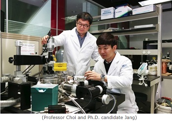
KAIST research team led by Professor Sung-Yool Choi at School of Electrical Engineering and Professor Sung Gap Im at the Department of Chemical and Biomolecular Engineering developed high-density, ultra-low power, non-volatile, flexible memory technology using 2D materials. The team used ultrathin molybdenum disulfide (MoS2) with atomic-scale thickness as the channel material and high-performance polymeric insulator film as the tunneling dielectric material. This research was published on the cover of Advanced Functional Materials on November 17. KAIST graduate Myung Hun Woo, a researcher at Samsung Electronics and Ph.D. candidate Byung Chul Jang are first authors.
The surge of new technologies such as Internet of Things (IoT), Artificial Intelligence (AI), and cloud server led to the paradigm shift from processor-centric computing to memory-centric computing in the industry, as well as the increase in demand of wearable devices. This led to an increased need for high-density, ultra-low power, non-volatile flexible memory. In particular, ultrathin MoS2 as semiconductor material has been recently regarded as post-silicon material. This is due to its ultrathin thickness of atomic-scale which suppresses short channel effect observed in conventional silicon material, leading to advantages in high- density and low-power consumption. Further, this thickness allows the material to be flexible, and thus the material is applicable to wearable devices.
Image caption: Concept map for the developed non-volatile memory material and high-resolution transmission electron microscopy image for material cross-section
However, due to the dangling-bond free surface of MoS2 semiconductor material, it is difficult to deposit the thin insulator film to be uniform and stable over a large area via the conventional atomic layer deposition process. Further, the currently used solution process makes it difficult to deposit uniformly low dielectric constant (k) polymeric insulator film with sub-10 nm thickness on a large area, thus indicating that the memory device utilizing the conventional solution-processed polymer insulator film cannot be operated at low-operating voltage and is not compatible with photolithography.
The research team tried to overcome the hurdles and develop high-density, ultra-low power, non-volatile flexible memory by employing a low-temperature, solvent-free, and all-dry vapor phase technique named initiated chemical vapor deposition (iCVD) process. Using iCVD process, tunneling polymeric insulator film with 10 nm thickness was deposited uniformly on MoS2 semiconductor material without being restricted by the dangling bond-free surface of MoS2. The team observed that the newly developed MoS2-based non-volatile memory can be operated at low-voltage (around 10V), in contrast to the conventional MoS2-based non-volatile memory that requires over 20V.
Professor Choi said, “As the basis for the Fourth Industrial revolution technologies including AI and IoT, semiconductor device technology needs to have characteristics of low-power and flexibility, in clear contrast to conventional memory devices.” He continued, “This new technology is significant in developing source technology in terms of materials, processes, and devices to contribute to achieve these characteristics.”
This research was supported by the Global Frontier Center for Advanced Soft Electronics and the Creative Materials Discovery Program by funded the National Research Foundation of Korea of Ministry of Science and ICT.
Share on:


Testimonial
"The I-Connect007 team is outstanding—kind, responsive, and a true marketing partner. Their design team created fresh, eye-catching ads, and their editorial support polished our content to let our brand shine. Thank you all! "
Sweeney Ng - CEE PCBSuggested Items
PC Graphics Add-in Board Shipments Up 27% QoQ in 2Q25
09/03/2025 | Jon Peddie ResearchAccording to a new research report from the analyst firm Jon Peddie Research, the growth of the global PC-based graphics add-in board market reached 11.6 million units in Q2'25 and desktop PC CPUs shipments increased to 21.7 million units.
PC GPU Shipments Up 8.4% in 2Q25 on Pre-Tariff Demand
09/02/2025 | Jon Peddie ResearchJon Peddie Research reports the growth of the global PC-based graphics processor unit (GPU) market reached 74.7 million units in Q2'25, and PC CPU shipments increased to 66.9 million units.
20 Years of Center Nanoelectronic Technologies (CNT) – Backbone of German Semiconductor Research Celebrates Anniversary
08/14/2025 | Fraunhofer IPMSThe Center Nanoelectronic Technologies (CNT) of the Fraunhofer Institute for Photonic Microsystems (IPMS) is celebrating its 20th anniversary this year. Since its founding in 2005, it has developed into a pillar of applied semiconductor research in Germany and Europe. With its unique research cleanroom and equipment adhering to the 300-mm wafer industry standard, CNT is unparalleled in Germany and serves as a central innovation driver for the microelectronics industry.
Q2 Client CPU Shipments Increased 8% from Last Quarter, Up 13% YoY
08/13/2025 | Jon Peddie ResearchJon Peddie Research reports that the global client CPU market expanded for two quarters in a row, and in Q2’25, it showed unseasonal growth of 7.9% from last quarter, while server CPU shipments increased 22% year over year.
FuriosaAI Closes $125M Investment Round to Scale Production of Next-Gen AI Inference Chip
07/31/2025 | BUSINESS WIREFuriosaAI, a semiconductor company building a new foundation for AI compute, today announced it has completed a $125 million Series C bridge funding round. The investment continues a period of significant momentum for Furiosa as global demand for high-performance, efficient AI infrastructure soars.