


 Defense Speak Interpreted: Extreme Financial Disparity in Drones and Missiles
 American Made Advocacy: Five Years of Educating, Advocating, and Influencing Legislation and Policy
 The Right Approach: The End of an Era—DoD Proposes MIL-PRF-31032 Cancellation


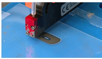
Researchers have developed a method to deposit tiny amounts of energetic materials (explosives, propellants, and pyrotechnics) using the same technology as an inkjet printer.
This research, which combines Purdue expertise in both energetic materials and additive manufacturing, allows energetic materials to be deposited with unprecedented levels of precision and safety.
“Energetic materials is a fairly understood field, and so is additive manufacturing,” said Allison Murray, a doctoral candidate in Purdue’s School of Mechanical Engineering, who built the custom inkjet printer. “What’s unique about this project is the intersection of those two fields and being able to safely deposit energetic materials with this level of precision.”
Many micromechanical systems incorporate energetic materials in their operation. For example, an automotive airbag deploys using a small amount of solid propellant. But as devices get smaller, the need for micro-level energetics becomes more critical.
“Our solution is to combine two components as we’re printing them,” said Jeff Rhoads, professor of mechanical engineering, and principal investigator on the project. “We can have a fuel and an oxidizer in two separate suspensions, which are largely inert. Then, with this custom inkjet printer, we can deposit the two in a specific overlapping pattern, combining them on a substrate to form nanothermite.”
“We’re talking about picoliters of material,” Murray said. “It was a challenge to get the right droplet volume and the right pattern.”
The other challenge: designing a machine that could deposit these droplets accurately. Murray’s machine holds the nozzle stationary and moves a stage below it to form whatever shape is required. “The stage can move with a 0.1 micron precision, which is basically a thousandth the width of a human hair,” she said.
The resulting nanothermite reacts just as quickly and powerfully as thermites applied in traditional ways.
“It burns at 2,500 Kelvin [over 4,000 degrees Fahrenheit],” Murray said. “It generates a lot of thrust, a lot of heat, and makes a nice loud shockwave.”
The project, which has been published in the Journal of Applied Physics, has a team of 10 researchers and four faculty members from varying disciplines in mechanical engineering. Rhoads studies micro-electromechanical systems; George Chiu is an expert in inkjet printing; and Emre Gunduz and Steve Son work at Zucrow Labs, studying energetic materials like explosives, propellants, and pyrotechnics.
“It’s a defining feature of Purdue that professors from such different backgrounds can work together on a project like this,” Rhoads said. “We can combine all of our experiences to collaborate on technologies that weren’t previously realizable.”


