


 Trouble in Your Tank: Implementing Direct Metallization in Advanced Substrate Packaging
 It’s Only Common Sense: Storytelling That Sells—Stop Pitching, Start Painting Pictures
 The Right Approach: Get Ready for ISO 9001 Version 6


Researchers Measure Single Atoms in a Graphene ‘Petri-Dish’
January 16, 2018 | University of ManchesterEstimated reading time: 2 minutes
Researchers working at The University of Manchester have shown new possibilities for observing nanomaterials in liquids by creating a graphene ‘petri-dish’.
New 2-dimensional nanomaterials have the potential to improve efficiencies, reduce costs and provide enhanced performance in a broad range of applications including; better design of nanomaterials for batteries or understanding the degradation of battery materials in order to improve their performance.
The unique properties exhibited by 2D materials could also lead to functional and antibacterial coatings, bioanalysis, and targeted drug delivery. However, the difficulty of controlling growth and degradation at the atomic scale is currently a hurdle to fully exploiting the potential of these exciting materials.
Scanning/transmission electron microscopy (S/TEM) is one of only few techniques that allows imaging and analysis of individual atoms. However, the S/TEM instrument requires a high vacuum to protect the electron source and to prevent electron scattering from molecular interactions.
Several high profile studies have previously revealed that the structure of functional materials at room temperature in a vacuum can significantly different from that in their normal liquid environment. This could be like trying to study the structure of a dehydrated prune to understand the structure of the original plum.
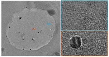
Publishing in Nano Letters, a research team led by Dr Sarah Haigh and Dr Roman Gorbachev at the National Graphene Institute and the School of Materials at The University of Manchester have shown that graphene and boron nitride can be combined to create a perfect nano petri-dish. Liquid samples inside the dish can be imaged with single atom sensitivity and it is also possible to measure their elemental composition at the nanometre length scale.
These engineered graphene liquid cells (EGLC) are built from 2D material-building blocks: they consist of a boron nitride (BN) spacer drilled with holes (where the liquid is contained) and encapsulated with graphene on both sides.
Graphene is the ultimate window material - strong enough to protect the sample from a high vacuum environment, but at the same time thin enough that the resolution of the electron beam is not compromised. Lead author Daniel Kelly said: “Unlike some previous designs our graphene liquid cells allow us to image the atoms for many minutes. We were even able to resolve individual atoms in water and observe them dancing under the electron beam.”
The researchers also demonstrated that these new graphene liquid cells enable an order of magnitude improvement in the quality of elemental analysis in liquid cells. They studied the deposition of a 1nm shell of iron on gold to grow core-shell nanoparticles. This new ability to monitor tiny concentrations over such small length-scales is a necessity for the increasingly complex chemical structures of high-performing nanocatalysts.
Mingwei Zhou, the student making these cells, said: “We are getting to understand how to make these more and more reliably, this makes the 2D petri-dish a promising route to further in situ TEM advancements, including imaging of small biological structures such as proteins.”
Share on:


Testimonial
"The I-Connect007 team is outstanding—kind, responsive, and a true marketing partner. Their design team created fresh, eye-catching ads, and their editorial support polished our content to let our brand shine. Thank you all! "
Sweeney Ng - CEE PCBSuggested Items
September PCB007 Magazine: The Future of Advanced Materials
09/16/2025 | I-Connect007 Editorial TeamMoore’s Law is no more, and the advanced material solutions being developed to grapple with this reality are surprising, stunning, and perhaps a bit daunting. Buckle up for a dive into advanced materials and a glimpse into the next chapters of electronics manufacturing.
I-Connect007 Launches Advanced Electronics Packaging Digest
09/15/2025 | I-Connect007I-Connect007 is pleased to announce the launch of Advanced Electronics Packaging Digest (AEPD), a new monthly digital newsletter dedicated to one of the most critical and rapidly evolving areas of electronics manufacturing: advanced packaging at the interconnect level.
Panasonic Industry will Double the Production Capacity of MEGTRON Multi-layer Circuit Board Materials Over the Next Five Years
09/15/2025 | Panasonic Industry Co., Ltd.Panasonic Industry Co., Ltd., a Panasonic Group company, announced plans for a major expansion of its global production capacity for MEGTRON multi-layer circuit board materials today. The company plans to double its production over the next five years to meet growing demand in the AI server and ICT infrastructure markets.
Trouble in Your Tank: Implementing Direct Metallization in Advanced Substrate Packaging
09/15/2025 | Michael Carano -- Column: Trouble in Your TankDirect metallization systems based on conductive graphite are gaining popularity throughout the world. The environmental and productivity gains achievable with this process are outstanding. Direct metallization reduces the costs of compliance, waste treatment, and legal issues related to chemical exposure. A graphite-based direct plate system has been devised to address these needs.
Fresh PCB Concepts: Designing for Success at the Rigid-flex Transition Area
08/28/2025 | Team NCAB -- Column: Fresh PCB ConceptsRigid-flex PCBs come in all shapes and sizes. Manufacturers typically use fire-retardant, grade 4 (FR-4) materials in the rigid section and flexible polyimide materials in the flex region. Because of the small size, some rigid-flex PCBs, like those for hearing aid devices, are among the most challenging to manufacture. However, regardless of its size, we should not neglect the transition area between the rigid and flexible material.