Ventec Passes AS9100 Revision D Transition Audit in China and UK
January 17, 2018 | Ventec International GroupEstimated reading time: 1 minute

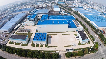
Ventec International Group is pleased to announce that the company headquarters in Suzhou, China and its European headquarters in the United Kingdom have both successfully passed the transition audit to AS9100 Revision D with zero non-conformances in accordance with the Aerospace Supplier Quality System Certification Scheme. SGS, the world's leading inspection, verification, testing and certification company have received recommendation to issue the upgrade certification to AS9100 Revision D for both locations.
With the transition audit passes to AS9100 Revision D at Ventec’s China and UK facilities, OEMs and PCB fabrication customers servicing the aviation, space and defense industries can continue to rely on Ventec's fully accredited supply chain for high reliability laminates and prepregs. From manufacture through fabrication and global delivery, Ventec's high quality product portfolio of polyimides, high reliability FR-4, tec-speed range of high speed/low loss materials and tec-thermal range of IMS materials are all covered by the accreditation.
Mark Goodwin, COO commented: “Achieving highest supply chain standards is paramount to our successful growth and I’m delighted with our recent successful re-certification audits in China and the UK. The results reflect the hard work of our entire team in implementing and practicing the highest levels of quality throughout our supply chain, enabling our PCB and OEM customers to engage Ventec as a strategic partner in their safety critical supply chains, based not just on the proven performance of our materials but on our commitment to managing delivered quality to the highest standards.”
About Ventec International
With volume manufacturing facilities and HQ in Suzhou China, Ventec International specializes in advanced copper clad glass reinforced and metal backed substrates for the PCB industry. With distribution locations and manufacturing sites in both the US and Europe, Ventec International is a premier supplier to the Global PCB industry. For more information, click here.
Testimonial
"The I-Connect007 team is outstanding—kind, responsive, and a true marketing partner. Their design team created fresh, eye-catching ads, and their editorial support polished our content to let our brand shine. Thank you all! "
Sweeney Ng - CEE PCBSuggested Items
Trouble in Your Tank: Implementing Direct Metallization in Advanced Substrate Packaging
09/15/2025 | Michael Carano -- Column: Trouble in Your TankDirect metallization systems based on conductive graphite are gaining popularity throughout the world. The environmental and productivity gains achievable with this process are outstanding. Direct metallization reduces the costs of compliance, waste treatment, and legal issues related to chemical exposure. A graphite-based direct plate system has been devised to address these needs.
Closing the Loop on PCB Etching Waste
09/09/2025 | Shawn Stone, IECAs the PCB industry continues its push toward greener, more cost-efficient operations, Sigma Engineering’s Mecer System offers a comprehensive solution to two of the industry’s most persistent pain points: etchant consumption and rinse water waste. Designed as a modular, fully automated platform, the Mecer System regenerates spent copper etchants—both alkaline and acidic—and simultaneously recycles rinse water, transforming a traditionally linear chemical process into a closed-loop system.
Driving Innovation: Depth Routing Processes—Achieving Unparalleled Precision in Complex PCBs
09/08/2025 | Kurt Palmer -- Column: Driving InnovationIn PCB manufacturing, the demand for increasingly complex and miniaturized designs continually pushes the boundaries of traditional fabrication methods, including depth routing. Success in these applications demands not only on robust machinery but also sophisticated control functions. PCB manufacturers rely on advanced machine features and process methodologies to meet their precise depth routing goals. Here, I’ll explore some crucial functions that empower manufacturers to master complex depth routing challenges.
Trouble in Your Tank: Minimizing Small-via Defects for High-reliability PCBs
08/27/2025 | Michael Carano -- Column: Trouble in Your TankTo quote the comedian Stephen Wright, “If at first you don’t succeed, then skydiving is not for you.” That can be the battle cry when you find that only small-diameter vias are exhibiting voids. Why are small holes more prone to voids than larger vias when processed through electroless copper? There are several reasons.
The Government Circuit: Navigating New Trade Headwinds and New Partnerships
08/25/2025 | Chris Mitchell -- Column: The Government CircuitAs global trade winds continue to howl, the electronics manufacturing industry finds itself at a critical juncture. After months of warnings, the U.S. Government has implemented a broad array of tariff increases, with fresh duties hitting copper-based products, semiconductors, and imports from many nations. On the positive side, tentative trade agreements with Europe, China, Japan, and other nations are providing at least some clarity and counterbalance.