


 Trouble in Your Tank: Implementing Direct Metallization in Advanced Substrate Packaging
 It’s Only Common Sense: Storytelling That Sells—Stop Pitching, Start Painting Pictures
 The Right Approach: Get Ready for ISO 9001 Version 6


Experiments Confirm First Chiral Phonon that Could Enable Exotic Forms of Electronics
February 2, 2018 | Lawrence Berkeley National LaboratoryEstimated reading time: 5 minutes
A research team from the Department of Energy’s Lawrence Berkeley National Laboratory (Berkeley Lab) has found the first evidence that a shaking motion in the structure of an atomically thin (2-D) material possesses a naturally occurring circular rotation.
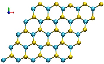
The atomic motion in a 2-D material, tungsten disulfide, is shown in this animation. In this phonon mode (known as longitudinal optical mode or LO), the selenium atoms (yellow) rotate clockwise while the tungsten atoms (blue) are still. (Credit: Hanyu Zhu, et al.)
This rotation could become the building block for a new form of information technology, and for the design of molecular-scale rotors to drive microscopic motors and machines.
The monolayer material, tungsten diselenide (WSe2), is already well-known for its unusual ability to sustain special electronic properties that are far more fleeting in other materials.
It is considered a promising candidate for a sought-after form of data storage known as valleytronics, for example, in which the momentum and wavelike motion of electrons in a material can be sorted into opposite “valleys” in a material’s electronic structure, with each of these valleys representing the ones and zeroes in conventional binary data.
Modern electronics typically rely on manipulations of the charge of electrons to carry and store information, though as electronics are increasingly miniaturized they are more subject to problems associated with heat buildup and electric leaks.
The latest study, published online this week in the journal Science, provides a possible path to overcome these issues. It reports that some of the material’s phonons, a term describing collective vibrations in atomic crystals, are naturally rotating in a certain direction.
This property is known as chirality – similar to a person’s handedness where the left and right hand are a mirror image of each other but not identical. Controlling the direction of this rotation would provide a stable mechanism to carry and store information.
“Phonons in solids are usually regarded as the collective linear motion of atoms,” said Xiang Zhang, the corresponding author of the study and senior scientist of the Materials Science Division at Lawrence Berkeley National Laboratory and professor at UC Berkeley. “Our experiment discovered a new type of so-called chiral phonons where atoms move in circles in an atomic monolayer crystal of tungsten diselenide.”
Hanyu Zhu, the lead author of the study and a postdoctoral researcher at Zhang’s group, said, “One of the biggest advantage of chiral phonon is that the rotation is locked with the particle’s momentum and not easily disturbed.”
In the phonon mode studied, the selenium atoms appear to collectively rotate in a clockwise direction, while the tungsten atoms showed no motion. Researchers prepared a “sandwich” with four sheets of centimeter-sized monolayer WSe2 samples placed between thin sapphire crystals. They synced ultrafast lasers to record the time-dependent motions.
The two laser sources converged on a spot on the samples measuring just 70 millionths of a meter in diameter. One of the lasers was precisely switched between two different tuning modes to sense the difference of left and right chiral phonon activity.
Image - This diagram shows atomic motion in separate phonon modes. At left ("LO" represents a longitudinal optical mode), selenium atoms exhibit a clockwise rotation while tungsten atoms stand still. At right ("LA" represents a longitudinal acoustic mode), tungsten atoms exhibit a clockwise rotation while selenium atoms rotate in a counterclockwise direction. (Credit: Hanyu Zhu, et al.)
This diagram maps out atomic motion in separate phonon modes. At left (“LO” represents a longitudinal optical mode), selenium atoms exhibit a clockwise rotation while tungsten atoms stand still. At right (“LA” represents a longitudinal acoustic mode), tungsten atoms exhibit a clockwise rotation while selenium atoms rotate in a counterclockwise direction. (Credit: Hanyu Zhu, et al.)
A so-called pump laser produced visible, red-light pulses that excited the samples, and a probe laser produced mid-infrared pulses that followed the first pump pulse within one trillionth of a second. About one mid-infrared photon in every 100 million is absorbed by WSe2 and converted to a chiral phonon.
The researchers then captured the high-energy luminescence from the sample, a signature of this rare absorption event. Through this technique, known as transient infrared spectroscopy, researchers not only confirmed the existence of a chiral phonon but also accurately obtained its rotational frequency.
So far, the process only produces a small number of chiral phonons. A next step in the research will be to generate larger numbers of rotating phonons, and to learn whether vigorous agitations in the crystal can be used to flip the spin of electrons or to significantly alter the valley properties of the material. Spin is an inherent property of an electron that can be thought of as its compass needle – if it could be flipped to point either north or south it could be used to convey information in a new form of electronics called spintronics.
“The potential phonon-based control of electrons and spins for device applications is very exciting and within reach,” Zhu said. “We already proved that phonons are capable of switching the electronic valley. In addition, this work allows the possibility of using the rotating atoms as little magnets to guide the spin orientation.”
The chiral properties found in the study likely exist across a wide range of 2-D materials based on a similar patterning in their atomic structure, Zhu also noted, adding that the study could guide theoretical investigations of electron-phonon interactions and the design of materials to enhance phonon-based effects.
“The same principle works in all 2-D periodic structures with three-fold symmetry and inversion asymmetry” Zhu said. “The same principle covers a huge family of natural materials, and there are almost infinite possibilities for creating rotors at the molecular scale.”
Researchers at UC Berkeley, King Abdullah University of Science and Technology in Saudi Arabia, and Nanjing Normal University in China also participated in the study. This work was primarily supported by the U.S. Department of Energy’s Office of Science.
About Lawrence Berkeley National Laboratory
Lawrence Berkeley National Laboratory addresses the world’s most urgent scientific challenges by advancing sustainable energy, protecting human health, creating new materials, and revealing the origin and fate of the universe. Founded in 1931, Berkeley Lab’s scientific expertise has been recognized with 13 Nobel Prizes. The University of California manages Berkeley Lab for the U.S. Department of Energy’s Office of Science.
Share on:


Testimonial
"The I-Connect007 team is outstanding—kind, responsive, and a true marketing partner. Their design team created fresh, eye-catching ads, and their editorial support polished our content to let our brand shine. Thank you all! "
Sweeney Ng - CEE PCBSuggested Items
I-Connect007 Launches Advanced Electronics Packaging Digest
09/15/2025 | I-Connect007I-Connect007 is pleased to announce the launch of Advanced Electronics Packaging Digest (AEPD), a new monthly digital newsletter dedicated to one of the most critical and rapidly evolving areas of electronics manufacturing: advanced packaging at the interconnect level.
Panasonic Industry will Double the Production Capacity of MEGTRON Multi-layer Circuit Board Materials Over the Next Five Years
09/15/2025 | Panasonic Industry Co., Ltd.Panasonic Industry Co., Ltd., a Panasonic Group company, announced plans for a major expansion of its global production capacity for MEGTRON multi-layer circuit board materials today. The company plans to double its production over the next five years to meet growing demand in the AI server and ICT infrastructure markets.
Trouble in Your Tank: Implementing Direct Metallization in Advanced Substrate Packaging
09/15/2025 | Michael Carano -- Column: Trouble in Your TankDirect metallization systems based on conductive graphite are gaining popularity throughout the world. The environmental and productivity gains achievable with this process are outstanding. Direct metallization reduces the costs of compliance, waste treatment, and legal issues related to chemical exposure. A graphite-based direct plate system has been devised to address these needs.
Fresh PCB Concepts: Designing for Success at the Rigid-flex Transition Area
08/28/2025 | Team NCAB -- Column: Fresh PCB ConceptsRigid-flex PCBs come in all shapes and sizes. Manufacturers typically use fire-retardant, grade 4 (FR-4) materials in the rigid section and flexible polyimide materials in the flex region. Because of the small size, some rigid-flex PCBs, like those for hearing aid devices, are among the most challenging to manufacture. However, regardless of its size, we should not neglect the transition area between the rigid and flexible material.
Global Sourcing Spotlight: How to Evaluate Supplier Capabilities Worldwide
08/20/2025 | Bob Duke -- Column: Global Sourcing SpotlightIn global sourcing, the difference between a competitive edge and a catastrophic disruption often comes down to how well you vet your suppliers. Sourcing advanced PCBs, precision components, or materials for complex assemblies demands diligence, skepticism, and more than a little time on airplanes. Here’s how to do your due diligence when evaluating international suppliers and why cutting corners can cost you more than money.