


 It’s Only Common Sense: The Importance of Setting Realistic Expectations
 Marcy’s Musings: The Relentless Pursuit of Perfection
 Dan’s Biz Bookshelf: ‘Do/Start'


Building Miniature Optical Antennas Using DNA as a Guide
February 5, 2018 | University of JyväskyläEstimated reading time: 2 minutes
A new fabrication technique combines programmable DNA origami shapes and conventional lithography methods to create metallic nanoantennas and chiral shapes for diverse applications.
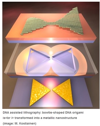
Research groups from University of Jyväskylä and Aalto University (Finland) together with researchers from California Institute of Technology (Caltech, USA) and Aarhus University (iNANO Center, Denmark) have reported a new highly parallel technique to fabricate precise metallic nanostructures with designed plasmonic properties by means of different self-assembled DNA origami shapes. The so-called DALI (DNA-assisted lithography) method has been published in the latest issue of Science Advances.
“We can build virtually any nanoscale shape using a DNA origami technique, and now we have shown how to use these accurate shapes as “stencils” to create millions of fully metallic nanostructures with 10 nm feature sizes in one go”, explains Adjunct Professor Veikko Linko from Aalto University. The trick in the DALI method is that when the DNA structures are deposited on a chip coated with silicon, silicon oxide can be selectively grown only on the bare areas of the substrate. “By controlling this process, we can create origami-shaped openings on the grown silicon oxide layer, and this layer can be used as a mask for the following lithography steps. Finally, we evaporate metal through these openings and create metallic structures having the same shape and size as the original DNA origami on a transparent substrate, such as sapphire”, Boxuan Shen from the Nanoscience Center of University of Jyväskylä describes the method.
The tiny metallic features cover the whole transparent substrate, and therefore these surfaces have intriguing optical properties. The small dimensions of the structures – in the range of ten nanometers – allow further tuning of these properties at the visible wavelength range. “Actually, we have demonstrated here a structure that we believe is the world’s smallest entirely metallic bowtie-shaped antenna. This extremely small size extends the operating range of optical features from infrared to visible”, states Adjunct Professor Jussi Toppari from Molecular Electronics and Plasmonics group at University of Jyväskylä. These antennas can find use in dozens of optical and plasmonic applications, such as surface enhanced Raman spectroscopy, biosensing or fluorescence enhancement. Moreover, the researchers demonstrated that the surfaces can be used as polarizers by fabricating chiral structures using DALI.
“The DALI method is highly parallel, and it could further enable cheap wafer-scale production of surfaces as it does not rely on costly patterning methods. It is also equipped for the future studies to provide bioinspired surfaces and metamaterials if the customized origami structures can be arranged on the substrate before metallization”, envisions Professor Mauri Kostiainen from the Biohybrid Materials Group at Aalto University.
Share on:


Suggested Items
Zhen Ding Reported Its 1Q25 Results, with Revenue Hitting a Record High for the Same Period
05/16/2025 | Zhen Ding TechnologyZhen Ding Technology Holding Limited a global leading PCB manufacturer, today announced its consolidated financial results for the first quarter of 2025.
Global SiC Substrate Revenue Declines 9% in 2024; Long-Term Demand Remains Strong as 8-Inch Roadmap Gains Momentum
05/12/2025 | TrendForceTrendForce’s latest research shows that weakening demand in the automotive and industrial sectors has slowed shipment growth for SiC substrates in 2024.
Zhen Ding Releases April 2025 Monthly Revenue Report
05/07/2025 | Zhen Ding TechnologyZhen Ding Technology Holding Limited, a global leading PCB manufacturer, reported April 2025 revenue of NT$13,589 million, up 22.90% YoY, marking a record high for the same period in the company’s history.
AT&S Starts High Volume Manufacturing at New Plant in Kulim/Malaysia
05/06/2025 | AT&SAT&S Austria Technologie & Systemtechnik (Malaysia) Sdn Bhd is ready to start high volume manufacturing at the new campus at Kulim Hi-Tech Park (KHTP) in the state of Kedah. AT&S Malaysia delivers high-end Integrated Circuit (IC) Substrates for AMD’s data center processors and other customers.
LG Innotek to Build FC-BGA into 700 Million USD Business with State-of-the-art Dream Factory
05/01/2025 | PR NewswireLG unveiled the Dream Factory, a hub for the production of FC-BGAs (Flip Chip Ball Grid Arrays), the company's next-generation growth engine, to the media for the first time and announced it on the 30th April.