


 Trouble in Your Tank: Implementing Direct Metallization in Advanced Substrate Packaging
 It’s Only Common Sense: Storytelling That Sells—Stop Pitching, Start Painting Pictures
 The Right Approach: Get Ready for ISO 9001 Version 6


Printable, Colorful Camouflage with Polymers
February 8, 2018 | ACSEstimated reading time: 1 minute
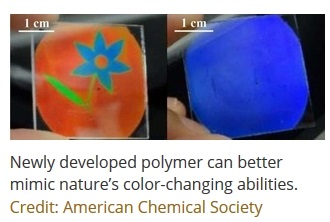
In nature, colors can serve as a form of communication, but they can also hide animals and plants, camouflaging them from sight. Researchers now report in ACS Applied Materials & Interfaces that they have developed polymers that can better mimic nature’s color-changing abilities than existing polymers. They say the materials could enable smart decorations, camouflage textiles and improved anti-counterfeiting measures.
Most of the colors that people are familiar with, such as hues on a piece of paper, are made with pigments. But another type, called structural color, exists, in which the color is produced by periodically arranged microscopic structures that interfere with visible light. For example, peacock tail feathers are actually brown, but microscopic structures present in the feathers make them look blue and green to the naked eye. Scientists have used cholesteric liquid-crystalline (CLC) polymers to mimic the structural coloration found in nature because they can easily be made into responsive materials. But so far, researchers have only produced them in a limited range of colors. So Albertus P. H. J. Schenning and Monali Moirangthem wanted to make CLC polymers with the full visible spectrum of colors.
The team used inkjet printing technology and a calcium nitrate solution to print an image on a CLC polymer they developed. Printing successive layers changed the degree of swelling of the CLC polymer, changing the color. One layer resulted in an orange color, a second layer changed it to green, and a third layer made it blue. As an example, the researchers used the method to draw a blue flower with green leaves on a reddish-orange background. After the ink dried, the image was no longer visible—the entire surface appeared blue. However, sprinkling water or breathing on it caused the full color image to re-appear.
Share on:


Testimonial
"The I-Connect007 team is outstanding—kind, responsive, and a true marketing partner. Their design team created fresh, eye-catching ads, and their editorial support polished our content to let our brand shine. Thank you all! "
Sweeney Ng - CEE PCBSuggested Items
U.S. Uses Secret Trackers to Trace AI Chips Diverted to China, Sources Say
08/18/2025 | I-Connect007 Editorial TeamTwo sources told Reuters that U.S. authorities have secretly placed location trackers in some advanced chip shipments they see as at high risk of illegal diversion to China. They said the trackers are intended to locate AI chips that are sent to locations restricted by U.S. export laws, but authorities only examine some shipments.
Happy’s Tech Talk #38: Novel Metallization for UHDI
05/07/2025 | Happy Holden -- Column: Happy’s Tech TalkI have been involved in high-density electronics substrates since 1970 when I joined Hewlett-Packard’s RF semiconductor group after college. Figure 1 shows the difference between trace/space lithography for substrates and silicon starting in 1970. My projects involved sapphire circuits for RF devices, but the figure displays the state of PCBs and integrated CMOS circuits and their packaging, not discreet RF devices. Even then, semiconductors were 50X higher density.
New Database of Materials Accelerates Electronics Innovation
05/05/2025 | ACN NewswireIn a collaboration between Murata Manufacturing Co., Ltd., and the National Institute for Materials Science (NIMS), researchers have built a comprehensive new database of dielectric material properties curated from thousands of scientific papers.
New Database of Materials Accelerates Electronics Innovation
05/02/2025 | ACN NewswireIn a collaboration between Murata Manufacturing Co., Ltd., and the National Institute for Materials Science (NIMS), researchers have built a comprehensive new database of dielectric material properties curated from thousands of scientific papers.
Micron Announces Business Unit Reorganization to Capitalize on AI Growth Across All Market Segments
04/23/2025 | MicronMicron Technology, Inc., a leader in innovative memory and storage solutions, announced a market segment-based reorganization of its business units to capitalize on the transformative growth driven by AI, from data centers to edge devices.