


 The Right Approach: Get Ready for ISO 9001 Version 6
 Dan’s Biz Bookshelf: ‘Still Broke: Walmart’s Remarkable Transformation'
 Driving Innovation: Depth Routing Processes—Achieving Unparalleled Precision in Complex PCBs


The Dawn of Gallium Oxide Microelectronics
February 9, 2018 | AIP.orgEstimated reading time: 2 minutes
Silicon has long been the go-to material in the world of microelectronics and semiconductor technology. But silicon still faces limitations, particularly with scalability for power applications. Pushing semiconductor technology to its full potential requires smaller designs at higher energy density.
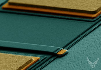
Image caption: A false-color, plan-view SEM image of a lateral gallium oxide field effect transistor with an optically defined gate. From near (bottom) to far (top): the source, gate, and drain electrodes. Metal is shown in yellow and orange, dark blue represents dielectric material, and lighter blue denotes the gallium oxide substrate. CREDIT: AFRL Sensors Directorate at WPAFB, Ohio, U.S.
“One of the largest shortcomings in the world of microelectronics is always good use of power: Designers are always looking to reduce excess power consumption and unnecessary heat generation,” said Gregg Jessen, principal electronics engineer at the Air Force Research Laboratory. “Usually, you would do this by scaling the devices. But the technologies in use today are already scaled close to their limits for the operating voltage desired in many applications. They are limited by their critical electric field strength.”
Transparent conductive oxides are a key emerging material in semiconductor technology, offering the unlikely combination of conductivity and transparency over the visual spectrum. One conductive oxide in particular has unique properties that allow it to function well in power switching: Ga2O3, or gallium oxide, a material with an incredibly large bandgap.
In their article published this week in Applied Physics Letters, from AIP Publishing, authors Masataka Higashiwaki and Jessen outline a case for producing microelectronics using gallium oxide. The authors focus on field effect transistors (FETs), devices that could greatly benefit from gallium oxide’s large critical electric field strength. a quality which Jessen said could enable the design of FETs with smaller geometries and aggressive doping profiles that would destroy any other FET material.
The material’s flexibility for various applications is due to its broad range of possible conductivities -- from highly conductive to very insulating -- and high-breakdown-voltage capabilities due to its electric field strength. Consequently, gallium oxide can be scaled to an extreme degree. Large-area gallium oxide wafers can also be grown from the melt, lowering manufacturing costs.
“The next application for gallium oxide will be unipolar FETs for power supplies,” Jessen said. “Critical field strength is the key metric here, and it results in superior energy density capabilities. The critical field strength of gallium oxide is more than 20 times that of silicon and more than twice that of silicon carbide and gallium nitride.”
The authors discuss manufacturing methods for Ga2O3 wafers, the ability to control electron density, and the challenges with hole transport. Their research suggests that unipolar Ga2O3 devices will dominate. Their paper also details Ga2O3 applications in different types of FETs and how the material can be of service in high-voltage, high-power and power-switching applications.
“From a research perspective, gallium oxide is really exciting,” Jessen said. “We are just beginning to understand the full potential of these devices for several applications, and it’s a great time to be involved in the field.”
Share on:


Testimonial
"Advertising in PCB007 Magazine has been a great way to showcase our bare board testers to the right audience. The I-Connect007 team makes the process smooth and professional. We’re proud to be featured in such a trusted publication."
Klaus Koziol - atgSuggested Items
Coherent Announces Agreement to Sell Aerospace and Defense Business to Advent for $400 Million
08/15/2025 | AdventCoherent Corp., a global leader in photonics, today announced that it has entered into a definitive agreement to sell its Aerospace and Defense business to Advent, a leading global private equity investor, for $400 million. Proceeds will be used to reduce debt, which will be immediately accretive to Coherent’s EPS.
Flexible Circuit Technologies to Host Free Flex Heater Webinar
08/18/2025 | Flexible Circuit TechnologiesGlobal Supplier of flexible circuits, flex design services, and assembly/box-build services, Flexible Circuit Technology will host their latest webinar, "Thermal Precision Meets Flexibility: The Technology Behind Heater Circuits" on Tuesday, August 26th, 2025 at 11 AM EDT.
Nordson Corporation Announces Earnings Release and Webcast for Third Quarter Fiscal Year 2025
07/31/2025 | Nordson CorporationNordson Corporation today announced it will release third quarter fiscal year 2025 earnings on August 20, 2025, after the close of the market.
Technica USA Welcomes Bill Dodd of Essemtec to the Bay Area
07/28/2025 | Technica USATechnica USA was pleased to welcome the good news regarding Essemtec’s decision to relocate Bill Dodd, Applications Engineer, from Boston to the Bay Area.
Knocking Down the Bone Pile: Tin Whisker Mitigation in Aerospace Applications, Part 3
06/25/2025 | Nash Bell -- Column: Knocking Down the Bone PileTin whiskers are slender, hair-like metallic growths that can develop on the surface of tin-plated electronic components. Typically measuring a few micrometers in diameter and growing several millimeters in length, they form through an electrochemical process influenced by environmental factors such as temperature variations, mechanical or compressive stress, and the aging of solder alloys.