


 Trouble in Your Tank: Implementing Direct Metallization in Advanced Substrate Packaging
 It’s Only Common Sense: Storytelling That Sells—Stop Pitching, Start Painting Pictures
 The Right Approach: Get Ready for ISO 9001 Version 6


Researchers Fabricate Trilayer Graphene with Different Electrical Properties
February 9, 2018 | Tohoku UniversityEstimated reading time: 2 minutes
Researchers in Japan have found a way to form two materials, each made of three layers of graphene. Each material's graphene is stacked differently and has unique electrical properties. Their work has implications for the development of novel electronic devices, such as photo sensors that convert light into electrical energy.
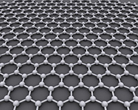
In 2004, two scientists realized they had isolated a single layer of carbon atoms on a scotch tape used to clean a graphite crystal. Since then, graphene has captured the imagination of researchers due to its fascinating properties: it is 200 times stronger than steel, is very flexible, and it is an excellent conductor of electricity.
The schematic crystal structures of (a) ABA- and (b) ABC- stacked three layer graphene.
Graphene's carbon atoms are arranged into hexagons, forming a honeycomb-like lattice. Placing one layer of graphene on top of another leads to the formation of bilayer graphene. The layers can be arranged in one of two positions: the centres of the carbon hexagons of each layer can be organized immediately above one another, called AA-stacking, or they can be displaced forwards so that a hexagon centre in one layer is above a carbon atom below it, called AB-stacking. AB-stacking of two layers of graphene leads to the formation of a material with semiconducting properties by applying an external electric field.
Deliberately stacking three layers of graphene has proven difficult. But doing so could help researchers study how the physical properties of tri-layered materials change based on how the layers are stacked. This could lead to the development of novel electrical devices.
Researchers at Japan's Tohoku University and Nagoya University have now fabricated two different types of trilayer graphene with different electrical properties.
They heated silicon carbide using one of two methods. In one experiment, silicon carbide was heated to 1,510°C under pressurized argon. In another, it was heated to 1,300°C in a high vacuum. Both materials were then sprayed with hydrogen gas in which the bonds were broken to form single hydrogen atoms. Two types of trilayer graphene then formed. The silicon carbide heated under pressurized argon formed into ABA-stacked graphene, in which the hexagons of the top and bottom layers were exactly aligned while the middle layer was slightly displaced. The silicon carbide heated in a vacuum developed into ABC-stacked graphene, in which each layer was slightly displaced in front of the one below it.
The researchers then examined the physical properties of each material and found that their electrons behaved differently. The ABA graphene was an excellent electrical conductor, similar to monolayer graphene. The ABC grapheme, on the other hand, acts more like AB graphene in that it had semi-conductor properties.
"The present success in selective fabrication of ABA and ABC trilayer graphene would widen the feasibility of graphene-based nano-electronic devices with variable layer numbers and stacking sequences," conclude the researchers in their study published in the journal NPG Asia Materials.
Share on:


Testimonial
"Advertising in PCB007 Magazine has been a great way to showcase our bare board testers to the right audience. The I-Connect007 team makes the process smooth and professional. We’re proud to be featured in such a trusted publication."
Klaus Koziol - atgSuggested Items
September PCB007 Magazine: The Future of Advanced Materials
09/16/2025 | I-Connect007 Editorial TeamMoore’s Law is no more, and the advanced material solutions being developed to grapple with this reality are surprising, stunning, and perhaps a bit daunting. Buckle up for a dive into advanced materials and a glimpse into the next chapters of electronics manufacturing.
I-Connect007 Launches Advanced Electronics Packaging Digest
09/15/2025 | I-Connect007I-Connect007 is pleased to announce the launch of Advanced Electronics Packaging Digest (AEPD), a new monthly digital newsletter dedicated to one of the most critical and rapidly evolving areas of electronics manufacturing: advanced packaging at the interconnect level.
Panasonic Industry will Double the Production Capacity of MEGTRON Multi-layer Circuit Board Materials Over the Next Five Years
09/15/2025 | Panasonic Industry Co., Ltd.Panasonic Industry Co., Ltd., a Panasonic Group company, announced plans for a major expansion of its global production capacity for MEGTRON multi-layer circuit board materials today. The company plans to double its production over the next five years to meet growing demand in the AI server and ICT infrastructure markets.
Trouble in Your Tank: Implementing Direct Metallization in Advanced Substrate Packaging
09/15/2025 | Michael Carano -- Column: Trouble in Your TankDirect metallization systems based on conductive graphite are gaining popularity throughout the world. The environmental and productivity gains achievable with this process are outstanding. Direct metallization reduces the costs of compliance, waste treatment, and legal issues related to chemical exposure. A graphite-based direct plate system has been devised to address these needs.
Fresh PCB Concepts: Designing for Success at the Rigid-flex Transition Area
08/28/2025 | Team NCAB -- Column: Fresh PCB ConceptsRigid-flex PCBs come in all shapes and sizes. Manufacturers typically use fire-retardant, grade 4 (FR-4) materials in the rigid section and flexible polyimide materials in the flex region. Because of the small size, some rigid-flex PCBs, like those for hearing aid devices, are among the most challenging to manufacture. However, regardless of its size, we should not neglect the transition area between the rigid and flexible material.