


 Trouble in Your Tank: Implementing Direct Metallization in Advanced Substrate Packaging
 It’s Only Common Sense: Storytelling That Sells—Stop Pitching, Start Painting Pictures
 The Right Approach: Get Ready for ISO 9001 Version 6


Scalable Two-Dimensional Materials Advance Future-Gen Electronics
February 15, 2018 | Pennsylvania State UniversityEstimated reading time: 3 minutes
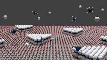
Since the discovery of the remarkable properties of graphene, scientists have increasingly focused research on the many other two-dimensional materials possible, both those found in nature and those concocted in the lab. However, growing high-quality, crystalline 2-D materials at scale has proven a significant challenge.
A pair of papers published online in two nanotechnology journals recently provide the basis for growing wafer-scale two-dimensional crystals for future electronic devices. In work led by Joan Redwing, director of the National Science Foundation-sponsored Two-Dimensional Crystal Consortium — Materials Innovation Platform, and professor of materials science and engineering and electrical engineering, Penn State, researchers developed a multistep process to make single crystal, atomically thin films of tungsten diselenide across large-area sapphire substrates.
"Up until now, the majority of 2-D devices have been fabricated using small flakes that are exfoliated off of bulk crystals," Redwing said. "To develop a device-ready technology, you have to be able to make devices on large-area substrates and they have to have good crystal quality."
The process uses sapphire as the substrate because of its crystalline structure. This structure orients the film growth in a crystal pattern in a process called epitaxy. As small islands of the material form on the substrate and the substrate is heated, the islands spread out across the substrate in a uniform pattern, forming a large-area film without gaps and with very few defects. The key advance was the use of gas-source chemical vapor deposition to precisely control the island density and rate of spreading to achieve a single layer of the 2-D material.
The researchers published their work, "Diffusion-Controlled Epitaxy of Large Area Coalesced WSe2 Monolayers on Sapphire," in Nano Letters.
In a related paper, "Realizing Large-Scale, Electronic-Grade Two-Dimensional Semiconductors," published online in ACS Nano, a team led by Joshua Robinson, associate professor of materials science and engineering, Penn State, provides the foundational understanding to enable device-ready synthetic 2-D semiconductors based on these epitaxial large-area films in future industrial-scale electronics.
"The primary significance of this work is we were able to achieve an understanding of the extrinsic factors that go into having a high-quality 2-D material," Robinson said. "What we found was that even when you grow oriented crystals on a surface, there are other factors that impact the ability to get high electron mobility or fast transistors."
In particular, they found that there is a strong interaction between the sapphire substrate and the monolayer film, with the substrate dominating the properties. To overcome these challenges, the researchers grew two or three layers, which improved the performance by factors of 20-100 times.
"This is the first real evidence of the effect of the substrate on the transport properties of 2-D layers," Robinson said.
Xiaotian Zhang, a doctoral student in Redwing's group, is first author on the Nano Letters paper. Yu-Chuan Lin, a former doctoral student in Robinson's group, is first author on the paper in ACS Nano. Both Redwing and Robinson are coauthors on both papers and are both members of the Materials Research Institute and the Penn State Two-Dimensional Crystal Consortium — Materials Innovation Platform, a National Science Foundation national user laboratory advancing the state-of-the art in the crystal growth of atomically thin 2-D materials for next-generation electronics (NSF cooperative agreement DMR-1539916).
The Dow Chemical Company, the Semiconductor Research Corporation through the Center for Low Energy Systems Technology (LEAST), and DARPA, the Defense Advanced Research Projects Administration, supported this work, in addition to NSF.
Twenty-two authors from four universities contributed to the ACS Nano paper, which reported on four years of research. Ten authors contributed to the Nano Letters paper, from both Penn State and Rensselaer Polytechnic Institute. Robinson would like to acknowledge Susan K. Fullerton's group from University of Pittsburgh for valuable contributions to the electrical section of the ACS Nano paper.
Share on:


Testimonial
"The I-Connect007 team is outstanding—kind, responsive, and a true marketing partner. Their design team created fresh, eye-catching ads, and their editorial support polished our content to let our brand shine. Thank you all! "
Sweeney Ng - CEE PCBSuggested Items
I-Connect007 Launches Advanced Electronics Packaging Digest
09/15/2025 | I-Connect007I-Connect007 is pleased to announce the launch of Advanced Electronics Packaging Digest (AEPD), a new monthly digital newsletter dedicated to one of the most critical and rapidly evolving areas of electronics manufacturing: advanced packaging at the interconnect level.
Panasonic Industry will Double the Production Capacity of MEGTRON Multi-layer Circuit Board Materials Over the Next Five Years
09/15/2025 | Panasonic Industry Co., Ltd.Panasonic Industry Co., Ltd., a Panasonic Group company, announced plans for a major expansion of its global production capacity for MEGTRON multi-layer circuit board materials today. The company plans to double its production over the next five years to meet growing demand in the AI server and ICT infrastructure markets.
Trouble in Your Tank: Implementing Direct Metallization in Advanced Substrate Packaging
09/15/2025 | Michael Carano -- Column: Trouble in Your TankDirect metallization systems based on conductive graphite are gaining popularity throughout the world. The environmental and productivity gains achievable with this process are outstanding. Direct metallization reduces the costs of compliance, waste treatment, and legal issues related to chemical exposure. A graphite-based direct plate system has been devised to address these needs.
Fresh PCB Concepts: Designing for Success at the Rigid-flex Transition Area
08/28/2025 | Team NCAB -- Column: Fresh PCB ConceptsRigid-flex PCBs come in all shapes and sizes. Manufacturers typically use fire-retardant, grade 4 (FR-4) materials in the rigid section and flexible polyimide materials in the flex region. Because of the small size, some rigid-flex PCBs, like those for hearing aid devices, are among the most challenging to manufacture. However, regardless of its size, we should not neglect the transition area between the rigid and flexible material.
Global Sourcing Spotlight: How to Evaluate Supplier Capabilities Worldwide
08/20/2025 | Bob Duke -- Column: Global Sourcing SpotlightIn global sourcing, the difference between a competitive edge and a catastrophic disruption often comes down to how well you vet your suppliers. Sourcing advanced PCBs, precision components, or materials for complex assemblies demands diligence, skepticism, and more than a little time on airplanes. Here’s how to do your due diligence when evaluating international suppliers and why cutting corners can cost you more than money.