


 Trouble in Your Tank: Implementing Direct Metallization in Advanced Substrate Packaging
 It’s Only Common Sense: Storytelling That Sells—Stop Pitching, Start Painting Pictures
 The Right Approach: Get Ready for ISO 9001 Version 6


A Quadrillionth of a Second in Slow Motion
February 22, 2018 | Max Planck Institute of Quantum OpticsEstimated reading time: 2 minutes
Many chemical processes run so fast that they are only roughly understood. To clarify these processes, a team from the Technical University of Munich (TUM) has now developed a methodology with a resolution of quintillionths of a second. The new technology stands to help better understand processes like photosynthesis and develop faster computer chips.
An important intermediary step in many chemical processes is ionization. A typical example of this is photosynthesis. The reactions run extremely fast. They take only a few femtoseconds (quadrillionths of a second) or even merely a few hundred attoseconds (quintillionths of a second). Because of these extremely short time scales, the initial and final products are known, but not the reaction paths or the intermediate products.
To observe such ultrafast processes, science needs a measurement technology that is faster than the observed process itself. So-called “pump and probe” spectroscopy makes this possible.
Here, the sample is excited using an initial laser pulse, which sets the reaction into motion. A second, time-delayed pulse queries the state of the sample at that moment. Multiple repetitions of the reaction with different time delays result in individual stop-motion images, which can then be compiled into a “film clip”.
Two Eyes See More Than One
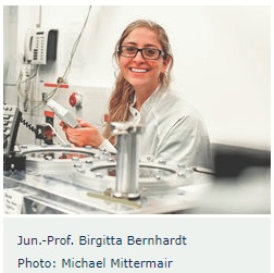
Now, a team of scientists headed by Birgitta Bernhardt, a former staff member at the Chair of Laser and X-ray Physics at TU Munich, who is now junior professor at the Institute of Applied Physics at the University of Jena, have for the first time succeeded in combining two pump and probe spectroscopy techniques using the inert gas krypton. This allowed them to shed light on the ultrafast ionization processes in a precision that has simply not been possible hitherto.
“Prior to our experiment, you could observe either which part of the exciting light was absorbed by the sample over time or measure what kind of and how many ions were created in the process,” explains Bernhardt. “We have now combined the two techniques, which allows us to observe the precise steps by which the ionization takes place, how long these intermediate products exist and what precisely the exciting laser pulse causes in the sample.”
Ultrafast Processes Under Control
The combination of the two measuring techniques allows the scientists not only to record the ultrafast ionization processes. Thanks to the variation in the intensity of the second, probing laser pulse, they can now, for the first time, also control and in this way also influence the ionization dynamics.
“This kind of control is a very powerful instrument,” explains Bernhardt. “If we can precisely understand and even influence fast ionization processes, we stand to learn a lot about light-driven processes like photosynthesis – especially about the initial moments in which this complex machinery is set into motion and which is hardly understood to date.”
Ultrafast Computers
The technology developed by Bernhardt and her colleagues is also interesting for the development of new, faster computer chips in which the ionization of silicon plays a significant role. If the ionization states of silicon can not only be sampled on such a short time scale, but can also be set – as the first experiments with krypton suggest – scientists might one day be able to use this to develop novel and even faster computer technologies.
Share on:


Testimonial
"The I-Connect007 team is outstanding—kind, responsive, and a true marketing partner. Their design team created fresh, eye-catching ads, and their editorial support polished our content to let our brand shine. Thank you all! "
Sweeney Ng - CEE PCBSuggested Items
Rules of Thumb: Design007 Magazine, November 2024
11/11/2024 | I-Connect007 Editorial TeamRules of thumb are everywhere, but there may be hundreds of rules of thumb for PCB design. They’re built on design formulas, fabricators’ limitations, and tribal knowledge. And unfortunately, some longtime rules of thumb should be avoided at all costs. How do we separate the wheat from the chaff, so to speak?
Connect the Dots: Best Practices for Prototyping
09/21/2023 | Matt Stevenson -- Column: Connect the DotsPCB prototyping is a critical juncture during an electronic device’s journey from concept to reality. Regardless of a project’s complexity, the process of transforming a design into a working board is often enlightening in terms of how a design can be improved before a PCB is ready for full production.
The Drive Toward UHDI and Substrates
09/20/2023 | I-Connect007 Editorial TeamPanasonic’s Darren Hitchcock spoke with the I-Connect007 Editorial Team on the complexities of moving toward ultra HDI manufacturing. As we learn in this conversation, the number of shifting constraints relative to traditional PCB fabrication is quite large and can sometimes conflict with each other.
Asia/Pacific AI Spending Surge to Reach a Projected $78 Billion by 2027
09/19/2023 | IDCAsia/Pacific spending on Artificial Intelligence (AI) ), including software, services, and hardware for AI-centric systems will grow to $78.4 billion in 2027, according to International Data Corporation's latest Worldwide Artificial Intelligence Spending Guide.
Intel to Sell Minority Stake in IMS Nanofabrication Business to TSMC
09/13/2023 | IntelIntel Corporation announced that it has agreed to sell an approximately 10% stake in the IMS Nanofabrication business to TSMC. TSMC’s investment values IMS at approximately $4.3 billion, consistent with the valuation of the recent stake sale to Bain Capital Special Situations.