


 Trouble in Your Tank: Implementing Direct Metallization in Advanced Substrate Packaging
 It’s Only Common Sense: Storytelling That Sells—Stop Pitching, Start Painting Pictures
 The Right Approach: Get Ready for ISO 9001 Version 6


Faster Data Transfer Through Plasmons
February 23, 2018 | A*STAREstimated reading time: 2 minutes
Photonic and electronic devices could soon be successfully integrated thanks to new transducers developed by a team of Singaporean researchers that can generate, manipulate and read small packets of energy called surface plasmon polaritons (SPPs).
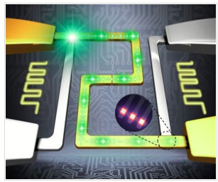
Image caption: This illustration shows two tunnel junctions coupled together by a plasmonic waveguide in the center. When a voltage is applied to the source junction, tunneling electrons excite surface plasmons, which propagate along the plasmonic waveguide and modulate the tunneling current at the detector junction. Inset: A light emission image of tunnel junctions, showing plasmons scattering from the end of the plasmonic waveguide. © 2018 Du Wei, National University of Singapore
Photonic devices, which use light rather than electric charges to carry information, can operate thousands of times faster than conventional electronics, although they tend to be large and difficult to integrate with microchips.
The team of researchers led by Hong-Son Chu at the A*STAR Institute of High Performance Computing and Christian Nijhuis at the National University of Singapore believe that SPPs, electromagnetic surface waves that exist at the interface of two materials, could be used to seamlessly link photonic devices and electronics.
“SPPs essentially contain light confined to dimensions smaller than its wavelength, and they function like photonic elements, carrying information at high speeds,” says Chu. “However, the SPPs offer the best of both worlds because they have the operational speed of optical elements as well as a small size suitable for nano-electronics applications. We have developed the first on-chip electronic-plasmonic transducers that operate at optical frequencies, and we achieved an electron-to-SPP conversion efficiency of more than 10 per cent.”
Most existing plasmonic devices require light sources such as LEDs to generate SPPs. This indirect method is quite slow. Chu and co-workers realized it would be much faster to produce SPPs by direct electrical means, so they designed transducers comprising aluminum and gold electrodes, separated by a two nanometer-thick layer of aluminum oxide that acts as an insulating ‘quantum tunneling’ barrier. Electrons that make the quantum leap across this gap will either generate or detect SPPs.
By joining two transducers with a plasmonic waveguide, so that one acted as a source and another as detector (see image), the researchers observed about 1 in 7 of the tunneling electrons coupling to a SPP. Although the reasons for this high tunneling rate are uncertain, Chu and co-workers suggest that SPPs at the junctions might induce an oscillating electric field, which changes the effective size of the tunneling gap and therefore the number of electrons that can cross the gap and interact with SPPs.
“By doing away with the need for light sources and detectors, devices based on this mechanism would be intrinsically fast,” says Chu. “Our work has attracted interest from research communities and industries, with potential applications in three-dimensional integrated circuits and high bandwidth memory devices. For example, there is a need for small, high-speed interconnectors to improve processing speeds.”
Share on:


Testimonial
"In a year when every marketing dollar mattered, I chose to keep I-Connect007 in our 2025 plan. Their commitment to high-quality, insightful content aligns with Koh Young’s values and helps readers navigate a changing industry. "
Brent Fischthal - Koh YoungSuggested Items
Advint Incorporated Brings Artificial Intelligence to Electroplating Training
09/11/2025 | Advint IncorporatedAdvint Incorporated is introducing a new dimension to its electroplating training programs: the integration of Artificial Intelligence (AI). This initiative reflects the company’s commitment to providing PCB fabricators and manufacturers in the USA and Canada with training that is practical, forward-looking, and directly relevant to today’s production challenges.
The Signal Integrity Issue: Design007 Magazine September 2025
09/09/2025 | I-Connect007 Editorial TeamAs the saying goes, “If you don’t have signal integrity problems now, you will eventually.” This month, our experts share a variety of design techniques that can help PCB designers and design engineers achieve signal integrity.
Semiconductors Get Magnetic Boost with New Method from UCLA Researchers
07/31/2025 | UCLA NewsroomA new method for combining magnetic elements with semiconductors — which are vital materials for computers and other electronic devices — was unveiled by a research team led by the California NanoSystems Institute at UCLA.
SMT Perspectives and Prospects: Warren Buffett’s Perpetual Wisdom, Part 1
07/29/2025 | Dr. Jennie Hwang -- Column: SMT Perspectives and ProspectsOver the years, I have cherished the lessons by Warren Buffett and Charlie Munger at the Berkshire Hathaway annual shareholders meeting in Omaha, Nebraska. This year, I was among the more than 40,000 who attended the May 3 meeting. Millions more from around the world, including from the UK, Germany, Japan, China, Panama, and Guatemala, tuned in remotely and via CNBC’s livestream.
Mesa West, Advanced West Announce Strategic Partnership
06/15/2025 | I-Connect007Mesa West is proud to announce that they have officially joined forces with Advanced West. This strategic partnership brings together two industry leaders, uniting strengths to better serve customers through enhanced capabilities, expanded offerings, and continued commitment to quality.