


 Trouble in Your Tank: Implementing Direct Metallization in Advanced Substrate Packaging
 It’s Only Common Sense: Storytelling That Sells—Stop Pitching, Start Painting Pictures
 The Right Approach: Get Ready for ISO 9001 Version 6


New Technique Allows Printing of Flexible, Stretchable Silver Nanowire Circuits
February 26, 2018 | North Carolina State UniversityEstimated reading time: 1 minute
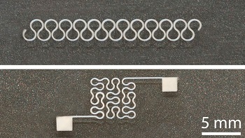
Researchers at North Carolina State University have developed a new technique that allows them to print circuits on flexible, stretchable substrates using silver nanowires. The advance makes it possible to integrate the material into a wide array of electronic devices.
Silver nanowires have drawn significant interest in recent years for use in many applications, ranging from prosthetic devices to wearable health sensors, due to their flexibility, stretchability and conductive properties. While proof-of-concept experiments have been promising, there have been significant challenges to printing highly integrated circuits using silver nanowires.
Silver nanoparticles can be used to print circuits, but the nanoparticles produce circuits that are more brittle and less conductive than silver nanowires. But conventional techniques for printing circuits don’t work well with silver nanowires; the nanowires often clog the printing nozzles.
“Our approach uses electrohydrodynamic printing, which relies on electrostatic force to eject the ink from the nozzle and draw it to the appropriate site on the substrate,” says Jingyan Dong, co-corresponding author of a paper on the work and an associate professor in NC State’s Edward P. Fitts Department of Industrial & Systems Engineering. “This approach allows us to use a very wide nozzle – which prevents clogging – while retaining very fine printing resolution.”
“And because our ‘ink’ consists of a solvent containing silver nanowires that are typically more than 20 micrometers long, the resulting circuits have the desired conductivity, flexibility and stretchability,” says Yong Zhu, a professor of mechanical engineering at NC State and co-corresponding author of the paper.
“In addition, the solvent we use is both nontoxic and water-soluble,” says Zheng Cui, a Ph.D. student at NC State and lead author of the paper. “Once the circuit is printed, the solvent can simply be washed off.”
What’s more, the size of the printing area is limited only by the size of the printer, meaning the technique could be easily scaled up.
The researchers have used the new technique to create prototypes that make use of the silver nanowire circuits, including a glove with an internal heater and a wearable electrode for use in electrocardiography. NC State has filed a provisional patent on the technique.
“Given the technique’s efficiency, direct writing capability, and scalability, we’re optimistic that this can be used to advance the development of flexible, stretchable electronics using silver nanowires – making these devices practical from a manufacturing perspective,” Zhu says.
Share on:


Testimonial
"We’re proud to call I-Connect007 a trusted partner. Their innovative approach and industry insight made our podcast collaboration a success by connecting us with the right audience and delivering real results."
Julia McCaffrey - NCAB GroupSuggested Items
Printed Electronics Market Size to Top $83.77 Billion by 2034 Driven by IoT Adoption and Flexible Device Demand
09/11/2025 | Globe NewswireThe printed electronics market size has been calculated at U$19,920 million in 2025 and is expected to grow from $23,58 million in 2026 to approximately $83,770 million by 2034.
Electroninks Acquires Complete UTDots Advanced Materials Nanoinks Portfolio and IP
05/19/2025 | ElectroninksElectroninks, the leader in metal organic decomposition (MOD) inks for additive manufacturing and advanced semiconductor packaging, announced it has officially completed its full acquisition of UTDots products and IP into its portfolio, further expanding its offerings in digital printing for high-performance applications.
Happy’s Tech Talk #38: Novel Metallization for UHDI
05/07/2025 | Happy Holden -- Column: Happy’s Tech TalkI have been involved in high-density electronics substrates since 1970 when I joined Hewlett-Packard’s RF semiconductor group after college. Figure 1 shows the difference between trace/space lithography for substrates and silicon starting in 1970. My projects involved sapphire circuits for RF devices, but the figure displays the state of PCBs and integrated CMOS circuits and their packaging, not discreet RF devices. Even then, semiconductors were 50X higher density.
Real Time with... IPC APEX EXPO 2025: Emerging Trends in Design and Technology
04/16/2025 | Real Time with...IPC APEX EXPOAndy Shaughnessy speaks with IPC design instructor Kris Moyer to discuss emerging design trends. They cover UHDI technology, 3D printing, and optical data transmission, emphasizing the importance of a skilled workforce. The role of AI in design is highlighted, along with the need for understanding physics and mechanics as designs become more complex. The conversation concludes with a focus on enhancing math skills for better signal integrity.
Real Time with... IPC APEX EXPO 2025: Transition Automation Focusing on Security Coatings and Squeegee Technology
04/16/2025 | Real Time with...IPC APEX EXPOMark Curtin, President of Transition Automation, gives an update on recent innovations at his company. He highlights a record sales month and their new focus on security coatings to fight counterfeiting. Mark explains the engineering behind their durable squeegees, the importance of maintenance, and the value of considering overall costs over just price.