


 It’s Only Common Sense: Marketing Isn’t Fluff, It’s Ammunition
 Driving Innovation: Mechanical and Optical Processes During Rigid-flex Production
 The Chemical Connection: Onshoring PCB Production—Daunting but Certainly Possible


Buckyball Marries Graphene
March 2, 2018 | Department of Energy, Office of ScienceEstimated reading time: 1 minute
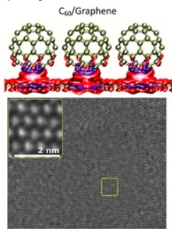
Electronic and structure richness arise from the merger of semiconducting molecules of carbon buckyballs and 2-D graphene.
Scientists combined buckyballs, which resemble tiny soccer balls made from 60 carbon atoms, with graphene, a single layer of carbon, on an underlying surface. Positive and negative charges can transfer between the balls and graphene depending on the nature of the surface as well as the structural order and local orientation of the carbon ball. Scientists can use this architecture to develop tunable junctions for lightweight electronic devices.
Fast-moving electrons and their counterpart, holes, were preserved in graphene with crystalline buckyball overlayers. Significantly, the carbon ball provides charge transfer to the graphene. Scientists expect the transfer to be highly tunable with external voltages. This marriage has ramifications for smart electronics that run longer and do not break as easily, bringing us closer to sensor-embedded smart clothing and robotic skin.
Charge transfer at the interface between dissimilar materials is at the heart of almost all electronic technologies such as transistors and photovoltaic devices. In this study, scientists studied charge transfer at the interface region of buckyball molecules deposited on graphene, with and without a supporting substrate, such as hexagonal boron nitride. They employed ab initio density functional theory with van der Waals interactions to model the structure theoretically. Van der Waals interactions are weak connections between neutral molecules. The team used high-resolution transmission electron microscopy and electronic transport measurements to characterize experimentally the properties of the interface.
The researchers observed that charge transfer between buckyballs and the graphene was sensitive to the nature of the underlying substrate, in addition, to the crystallinity and local orientation of the buckyballs. These studies open an avenue to devices where buckyball layers on top of graphene can serve as electron acceptors and other buckyball layers as electron donors. Even at room temperature, buckyball molecules were orientationally locked into position. This is in sharp contrast to buckyball molecules in un-doped bulk crystalline configurations, where locking occurs only at low temperature. High electron and hole mobilities are preserved in graphene with crystalline buckyball overlayers. This finding has ramifications for the development of organic high-mobility field-effect devices and other high mobility applications.
Share on:


Testimonial
"Our marketing partnership with I-Connect007 is already delivering. Just a day after our press release went live, we received a direct inquiry about our updated products!"
Rachael Temple - AlltematedSuggested Items
Infinite Electronics, RS Group Expand Partnership to Deliver L-com Connectivity Solutions to European and APAC Markets
11/03/2025 | PRNewswireL-com, an Infinite Electronics brand and a supplier of wired and wireless connectivity products, has expanded their strategic cooperation agreement with RS Group, a U.K.-based global provider of products and services for industrial customers, to begin distributing L-com products across European and APAC markets via the RS Group website.
DuPont Completes Separation of Qnity Electronics
11/03/2025 | PRNewswireDuPont announced that it completed the separation of its electronics business into an independent public company, Qnity Electronics, Inc., on November 1, 2025.
TTM Technologies Receives Two Awards from the Global Electronics Association at the 2025 IPC CEMAC Conference
11/03/2025 | Globe NewswireTTM Technologies, Inc. announced that two of its team members received prestigious Asia Steering Committee Outstanding Service Awards from the Global Electronics Association (formerly named IPC connecting global electronics industry) at the 2025 IPC CEMAC Electronics Manufacturing Annual Conference in Shanghai.
Ethiopian Airlines Selects Cassiopée Alpha from Safran for Fleet-wide Flight Data Monitoring
11/03/2025 | SafranSafran Electronics & Defense is proud to announce that Ethiopian Airlines has selected Cassiopée Alpha, its advanced flight data analysis platform, to optimize and secure operations across the airline’s entire fleet of 147 aircraft, including Airbus A350, Boeing 787, and Boeing 737 MAX models.
SMT007 Magazine November 2025: Inside Mexico’s Rise as an Electronics Manufacturing Leader
11/03/2025 | I-Connect007 Editorial TeamMexico isn’t just part of the electronics manufacturing conversation—it’s leading it. From growing investments to cross-border collaborations, Mexico is fast becoming the center of electronics in North America. In this issue, we uncover why Mexico is earning global recognition. From top-ranked manufacturing capabilities to expanding partnerships that reach far beyond the U.S.