


 Trouble in Your Tank: Implementing Direct Metallization in Advanced Substrate Packaging
 It’s Only Common Sense: Storytelling That Sells—Stop Pitching, Start Painting Pictures
 The Right Approach: Get Ready for ISO 9001 Version 6


Rice Team Designs Lens-Free Fluorescent Microscope
March 9, 2018 | Rice UniversityEstimated reading time: 4 minutes
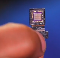
Lenses are no longer necessary for some microscopes, according to Rice University engineers developing FlatScope, a thin fluorescent microscope whose abilities promise to surpass those of old-school devices.
A paper in Science Advances by Rice engineers Ashok Veeraraghavan, Jacob Robinson, Richard Baraniuk and their labs describes a wide-field microscope thinner than a credit card, small enough to sit on a fingertip and capable of micrometer resolution over a volume of several cubic millimeters.
FlatScope eliminates the tradeoff that hinders traditional microscopes in which arrays of lenses can either gather less light from a large field of view or gather more light from a smaller field.
The Rice team began developing the device as part of a federal initiative by the Defense Advanced Research Projects Agency as an implantable, high-resolution neural interface. But the device’s potential is much greater. The researchers claim FlatScope, an advance on the labs’ earlier FlatCam, could be used as an implantable endoscope, a large-area imager or a flexible microscope.
“We think of this as amping up FlatCam so it can solve even bigger problems,” Baraniuk said.
Traditional fluorescent microscopes are essential tools in biology. They pick up fluorescent signals from particles inserted into cells and tissues that are illuminated with specific wavelengths of light. The technique allows scientists to probe and track biological agents with nanometer-scale resolution.
But like all traditional microscopes, telescopes and cameras, their resolution depends on the size of their lenses, which can be large and heavy and limit their use in biological applications.
The Rice team takes a different approach. It uses the same complementary metal–oxide–semiconductor (CMOS) chips found in all electronic cameras to capture incoming light, but the comparisons stop there. Like the FlatCam project that inspired it, FlatScope’s field of view equals the size of the CCD sensor, which can be as large or as small as required. It’s flat because it replaces the array of lenses in a traditional microscope with a custom amplitude mask.
This mask, which resembles a bar code, sits directly in front of the CCD. Light that comes through the mask and hits the sensor becomes data that a computer program interprets to produce images.
The algorithm can focus on any part of the three-dimensional data the scope captures and produce images of objects smaller than a micron anywhere in the field.
That resolution is what makes the device a microscope, Robinson said. “A camera in your mobile phone or DSLR typically gets on the order of 100-micron resolution,” he said. “When you take a macro photo, the resolution is about 20 to 50 microns.
“I think of a microscope as something that allows you to image things on the micron scale,” he said. “That means things that are smaller than the diameter of a human hair, like cells, parts of cells or the fine structure of fibers.”
Achieving that resolution required modifications to the FlatCam mask to further cut the amount of light that reaches the sensor as well as a rewrite of their software, Robinson said. “It wasn’t as trivial as simply applying the FlatCam algorithm to the same techniques we used to image things that are far away,” he said.
The mask is akin to the aperture in a lensed camera that focuses light onto the sensor, but it’s only a few hundred micrometers from the sensor and allows only a fraction of the available light to get through, limiting the amount of data to simplify processing.
“In the case of a megapixel camera, that computational problem requires a matrix of a million times a million elements,” Robinson said. “It’s an incredibly big matrix. But because we break it down through this pattern of rows and columns, our matrix is just 1 million elements.”
That cuts the data for each snapshot from six terabytes to a more practical 21 megabytes, which translates to short processing times. From early versions of FlatCam that required an hour or more to process an image, FlatScope captures 30 frames of 3-D data per second.
Veeraraghavan said the burgeoning internet of things may provide many applications for flat cameras and microscopes. That in turn would drive down costs. “One of the big advantages of this technology compared with traditional cameras is that because we don’t need lenses, we don’t need postfabrication assembly,” he said. “We can imagine this rolling off a fabrication line.”
But their primary targets are medical uses, from implantable scopes for the clinic to palm-sized microscopes for the battlefield. “To be able to carry a microscope in your pocket is a neat technology,” Veeraraghavan said.
The researchers noted that while their current work is focused on fluorescent applications, FlatScope could also be used for bright-field, dark-field and reflected-light microscopy. They suggested an array of FlatScopes on a flexible background could be used to match the contours of a target.
Rice graduate students Jesse Adams and Vivek Boominathan are lead authors of the paper. Co-authors are graduate students Daniel Vercosa and Fan Ye. Baraniuk is the Victor E. Cameron Professor of Electrical and Computer Engineering. Robinson is an assistant professor, and Veeraraghavan is an associate professor of electrical and computer engineering.
The National Science Foundation and the Defense Advanced Research Projects Agency funded the research.
Share on:


Testimonial
"Our marketing partnership with I-Connect007 is already delivering. Just a day after our press release went live, we received a direct inquiry about our updated products!"
Rachael Temple - AlltematedSuggested Items
Rules of Thumb: Design007 Magazine, November 2024
11/11/2024 | I-Connect007 Editorial TeamRules of thumb are everywhere, but there may be hundreds of rules of thumb for PCB design. They’re built on design formulas, fabricators’ limitations, and tribal knowledge. And unfortunately, some longtime rules of thumb should be avoided at all costs. How do we separate the wheat from the chaff, so to speak?
Connect the Dots: Best Practices for Prototyping
09/21/2023 | Matt Stevenson -- Column: Connect the DotsPCB prototyping is a critical juncture during an electronic device’s journey from concept to reality. Regardless of a project’s complexity, the process of transforming a design into a working board is often enlightening in terms of how a design can be improved before a PCB is ready for full production.
The Drive Toward UHDI and Substrates
09/20/2023 | I-Connect007 Editorial TeamPanasonic’s Darren Hitchcock spoke with the I-Connect007 Editorial Team on the complexities of moving toward ultra HDI manufacturing. As we learn in this conversation, the number of shifting constraints relative to traditional PCB fabrication is quite large and can sometimes conflict with each other.
Asia/Pacific AI Spending Surge to Reach a Projected $78 Billion by 2027
09/19/2023 | IDCAsia/Pacific spending on Artificial Intelligence (AI) ), including software, services, and hardware for AI-centric systems will grow to $78.4 billion in 2027, according to International Data Corporation's latest Worldwide Artificial Intelligence Spending Guide.
Intel to Sell Minority Stake in IMS Nanofabrication Business to TSMC
09/13/2023 | IntelIntel Corporation announced that it has agreed to sell an approximately 10% stake in the IMS Nanofabrication business to TSMC. TSMC’s investment values IMS at approximately $4.3 billion, consistent with the valuation of the recent stake sale to Bain Capital Special Situations.