


 Trouble in Your Tank: Implementing Direct Metallization in Advanced Substrate Packaging
 It’s Only Common Sense: Storytelling That Sells—Stop Pitching, Start Painting Pictures
 The Right Approach: Get Ready for ISO 9001 Version 6


OLED: Nanometer-thin Layer Improves Efficiency
March 13, 2018 | Max Planck Institute for Polymer ResearchEstimated reading time: 1 minute
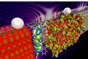
Scientists at the Max Planck Institute for Polymer Research in Mainz, Germany, have received an unexpected result: They have discovered a new method to improve contacts in OLEDs. This new approach leads to a higher energy efficiency and can be used in almost any organic semiconductor element.
Organic light-emitting diodes (OLEDs) are used as light sources in high-quality smartphone displays and large-area high-end products such as OLED televisions. The main active component in an OLED is a light-emitting layer of an organic semiconductor, which converts electrical energy into visible light. In an OLED, the organic semiconducting layer is situated between two electrodes; by applying a voltage across these two electrodes, an electric current passes through the OLED, which is converted into visible light.
However, for many organic semiconductors, especially for blue- or ultraviolet-emitting materials, it is difficult to inject the current from the positive electrode into the OLED. This leads to low efficiencies in OLEDs.
Dr. Gert-Jan Wetzelaer, Group Leader at the Max Planck Institute for Polymer Research in Mainz, Germany, has recently discovered a way of improving the current injection from the positive electrode in OLEDs. Wetzelaer and his team have covered the positive electrode with an ultrathin layer of another organic semiconductor as a spacer layer between the electrode and the light-emitting organic semiconductor. Wetzelaer said: “The result was unexpected. This nanometer-thin layer facilitates charge transfer between the electrode and the organic semiconductor. Although it seems to be illogical at first, eliminating physical contact between electrode and semiconductor actually improves the electrical contact.”
Improved Contacts in Semiconductors
Improving electrical contact with an ultrathin interlayer greatly increases the efficiency of ultraviolet-emitting OLEDs. The scientists at the MPI for Polymer Research have demonstrated this improvement of electrodes for a large number of organic semiconductors and for different spacer layers. Professor Paul Blom, Director at the Max Planck Institute for Polymer Research and head of its Molecular Electronics Department, is convinced: “This simple method of covering electrodes in OLEDs with an ultrathin layer for current-injection improvement is a resounding success for technical application in high-end electronics.”
Gert-Jan Wetzelaer and his research team are very confident that this new approach for fabricating improved contacts can be used in basically any organic-semiconductor device, which could boost their performance now.
Share on:


Testimonial
"The I-Connect007 team is outstanding—kind, responsive, and a true marketing partner. Their design team created fresh, eye-catching ads, and their editorial support polished our content to let our brand shine. Thank you all! "
Sweeney Ng - CEE PCBSuggested Items
PC Graphics Add-in Board Shipments Up 27% QoQ in 2Q25
09/03/2025 | Jon Peddie ResearchAccording to a new research report from the analyst firm Jon Peddie Research, the growth of the global PC-based graphics add-in board market reached 11.6 million units in Q2'25 and desktop PC CPUs shipments increased to 21.7 million units.
PC GPU Shipments Up 8.4% in 2Q25 on Pre-Tariff Demand
09/02/2025 | Jon Peddie ResearchJon Peddie Research reports the growth of the global PC-based graphics processor unit (GPU) market reached 74.7 million units in Q2'25, and PC CPU shipments increased to 66.9 million units.
20 Years of Center Nanoelectronic Technologies (CNT) – Backbone of German Semiconductor Research Celebrates Anniversary
08/14/2025 | Fraunhofer IPMSThe Center Nanoelectronic Technologies (CNT) of the Fraunhofer Institute for Photonic Microsystems (IPMS) is celebrating its 20th anniversary this year. Since its founding in 2005, it has developed into a pillar of applied semiconductor research in Germany and Europe. With its unique research cleanroom and equipment adhering to the 300-mm wafer industry standard, CNT is unparalleled in Germany and serves as a central innovation driver for the microelectronics industry.
Q2 Client CPU Shipments Increased 8% from Last Quarter, Up 13% YoY
08/13/2025 | Jon Peddie ResearchJon Peddie Research reports that the global client CPU market expanded for two quarters in a row, and in Q2’25, it showed unseasonal growth of 7.9% from last quarter, while server CPU shipments increased 22% year over year.
FuriosaAI Closes $125M Investment Round to Scale Production of Next-Gen AI Inference Chip
07/31/2025 | BUSINESS WIREFuriosaAI, a semiconductor company building a new foundation for AI compute, today announced it has completed a $125 million Series C bridge funding round. The investment continues a period of significant momentum for Furiosa as global demand for high-performance, efficient AI infrastructure soars.