


 Trouble in Your Tank: Implementing Direct Metallization in Advanced Substrate Packaging
 It’s Only Common Sense: Storytelling That Sells—Stop Pitching, Start Painting Pictures
 The Right Approach: Get Ready for ISO 9001 Version 6


‘Sweet Spot’ in Sweet Material for Hydrogen Storage
March 13, 2018 | Rice UniversityEstimated reading time: 4 minutes
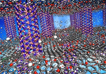
Rice University engineers have zeroed in on the optimal architecture for storing hydrogen in “white graphene” nanomaterials — a design like a Lilliputian skyscraper with “floors” of boron nitride sitting one atop another and held precisely 5.2 angstroms apart by boron nitride pillars.
Image caption: Thousands of hours of calculations on Rice University’s two fastest supercomputers found that the optimal architecture for packing hydrogen into “white graphene” involves making skyscraper-like frameworks of vertical columns and one-dimensional floors that are about 5.2 angstroms apart. In this illustration, hydrogen molecules (white) sit between sheet-like floors of graphene (gray) that are supported by boron-nitride pillars (pink and blue). Researchers found that identical structures made wholly of boron-nitride had unprecedented capacity for storing readily available hydrogen. (Credit: Lei Tao/Rice University)
“The motivation is to create an efficient material that can take up and hold a lot of hydrogen — both by volume and weight — and that can quickly and easily release that hydrogen when it’s needed,” said the study’s lead author, Rouzbeh Shahsavari, assistant professor of civil and environmental engineering at Rice.
Hydrogen is the lightest and most abundant element in the universe, and its energy-to-mass ratio — the amount of available energy per pound of raw material, for example — far exceeds that of fossil fuels. It’s also the cleanest way to generate electricity: The only byproduct is water. A 2017 report by market analysts at BCC Research found that global demand for hydrogen storage materials and technologies will likely reach $5.4 billion annually by 2021.
Hydrogen’s primary drawbacks relate to portability, storage and safety. While large volumes can be stored under high pressure in underground salt domes and specially designed tanks, small-scale portable tanks — the equivalent of an automobile gas tank — have so far eluded engineers.
Following months of calculations on two of Rice’s fastest supercomputers, Shahsavari and Rice graduate student Shuo Zhao found the optimal architecture for storing hydrogen in boron nitride. One form of the material, hexagonal boron nitride (hBN), consists of atom-thick sheets of boron and nitrogen and is sometimes called white graphene because the atoms are spaced exactly like carbon atoms in flat sheets of graphene.
Previous work in Shahsavari’s Multiscale Materials Lab found that hybrid materials of graphene and boron nitride could hold enough hydrogen to meet the Department of Energy’s storage targets for light-duty fuel cell vehicles.
“The choice of material is important,” he said. “Boron nitride has been shown to be better in terms of hydrogen absorption than pure graphene, carbon nanotubes or hybrids of graphene and boron nitride.
“But the spacing and arrangement of hBN sheets and pillars is also critical,” he said. “So we decided to perform an exhaustive search of all the possible geometries of hBN to see which worked best. We also expanded the calculations to include various temperatures, pressures and dopants, trace elements that can be added to the boron nitride to enhance its hydrogen storage capacity.”
Zhao and Shahsavari set up numerous “ab initio” tests, computer simulations that used first principles of physics. Shahsavari said the approach was computationally intense but worth the extra effort because it offered the most precision.
“We conducted nearly 4,000 ab initio calculations to try and find that sweet spot where the material and geometry go hand in hand and really work together to optimize hydrogen storage,” he said.
Unlike materials that store hydrogen through chemical bonding, Shahsavari said boron nitride is a sorbent that holds hydrogen through physical bonds, which are weaker than chemical bonds. That’s an advantage when it comes to getting hydrogen out of storage because sorbent materials tend to discharge more easily than their chemical cousins, Shahsavari said.
He said the choice of boron nitride sheets or tubes and the corresponding spacing between them in the superstructure were the key to maximizing capacity.
“Without pillars, the sheets sit naturally one atop the other about 3 angstroms apart, and very few hydrogen atoms can penetrate that space,” he said. “When the distance grew to 6 angstroms or more, the capacity also fell off. At 5.2 angstroms, there is a cooperative attraction from both the ceiling and floor, and the hydrogen tends to clump in the middle. Conversely, models made of purely BN tubes — not sheets — had less storage capacity.”
Shahsavari said models showed that the pure hBN tube-sheet structures could hold 8 weight percent of hydrogen. (Weight percent is a measure of concentration, similar to parts per million.) Physical experiments are needed to verify that capacity, but that the DOE’s ultimate target is 7.5 weight percent, and Shahsavari’s models suggests even more hydrogen can be stored in his structure if trace amounts of lithium are added to the hBN.
Finally, Shahsavari said, irregularities in the flat, floor-like sheets of the structure could also prove useful for engineers.
“Wrinkles form naturally in the sheets of pillared boron nitride because of the nature of the junctions between the columns and floors,” he said. “In fact, this could also be advantageous because the wrinkles can provide toughness. If the material is placed under load or impact, that buckled shape can unbuckle easily without breaking. This could add to the material’s safety, which is a big concern in hydrogen storage devices.
“Furthermore, the high thermal conductivity and flexibility of BN may provide additional opportunities to control the adsorption and release kinetics on-demand,” Shahsavari said. “For example, it may be possible to control release kinetics by applying an external voltage, heat or an electric field.”
Share on:


Testimonial
"The I-Connect007 team is outstanding—kind, responsive, and a true marketing partner. Their design team created fresh, eye-catching ads, and their editorial support polished our content to let our brand shine. Thank you all! "
Sweeney Ng - CEE PCBSuggested Items
I-Connect007 Launches Advanced Electronics Packaging Digest
09/15/2025 | I-Connect007I-Connect007 is pleased to announce the launch of Advanced Electronics Packaging Digest (AEPD), a new monthly digital newsletter dedicated to one of the most critical and rapidly evolving areas of electronics manufacturing: advanced packaging at the interconnect level.
Panasonic Industry will Double the Production Capacity of MEGTRON Multi-layer Circuit Board Materials Over the Next Five Years
09/15/2025 | Panasonic Industry Co., Ltd.Panasonic Industry Co., Ltd., a Panasonic Group company, announced plans for a major expansion of its global production capacity for MEGTRON multi-layer circuit board materials today. The company plans to double its production over the next five years to meet growing demand in the AI server and ICT infrastructure markets.
Trouble in Your Tank: Implementing Direct Metallization in Advanced Substrate Packaging
09/15/2025 | Michael Carano -- Column: Trouble in Your TankDirect metallization systems based on conductive graphite are gaining popularity throughout the world. The environmental and productivity gains achievable with this process are outstanding. Direct metallization reduces the costs of compliance, waste treatment, and legal issues related to chemical exposure. A graphite-based direct plate system has been devised to address these needs.
Integrated Solutions for Board-level Reliability: A Smarter Path Forward
08/27/2025 | Alan Gardner, MacDermid Alpha Electronics SolutionsIn today’s electronics manufacturing landscape, reliability is no longer just a benchmark but a business imperative. As industries such as automotive, aerospace, and high-performance computing (HPC) push the boundaries of innovation, the demand for dependable board-level performance under extreme conditions has never been greater.
Fresh PCB Concepts: Designing for Success at the Rigid-flex Transition Area
08/28/2025 | Team NCAB -- Column: Fresh PCB ConceptsRigid-flex PCBs come in all shapes and sizes. Manufacturers typically use fire-retardant, grade 4 (FR-4) materials in the rigid section and flexible polyimide materials in the flex region. Because of the small size, some rigid-flex PCBs, like those for hearing aid devices, are among the most challenging to manufacture. However, regardless of its size, we should not neglect the transition area between the rigid and flexible material.