


 Trouble in Your Tank: Implementing Direct Metallization in Advanced Substrate Packaging
 It’s Only Common Sense: Storytelling That Sells—Stop Pitching, Start Painting Pictures
 The Right Approach: Get Ready for ISO 9001 Version 6


NPL Scientists Create Diodes Made of Light
March 16, 2018 | National Physical LaboratoryEstimated reading time: 2 minutes
Photonics researchers at the National Physical Laboratory (NPL) have achieved the extra-ordinary by creating a diode consisting of light that can be used, for the first time, in miniaturised photonic circuits, as published in Optica.
NPL Scientists Create Diodes Made of Light
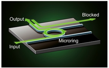
Concept of the microring diode. Light is transmitted from 'Input' to 'Output' through a microring resonator. Light-with-light interaction in the microring blocks backwards propagating light from entering the ring.
Dr. Pascal Del'Haye and his team at NPL have created an optical version of a diode that transmits light in one direction only, and can be integrated in microphotonic circuits. This small-scale integration has been a major challenge in photonics because existing optical diodes require bulky magnets.
NPL's ground-breaking work has overcome the limitation of diodes based on bulky magnets, by using light stored in tiny chip-based glass rings to form a diode.
Diodes are well known in electronic circuits. They transmit electric current in one direction but block the current in the backward direction. Diodes are essential components of nearly every electronic circuit and are used, for example, in battery chargers.
The novel technique was created by sending lots of light into a microresonator – a glass ring on a silicon chip, about the width of a human hair – and harnessing the circulating optical power to generate the diode effect.
Dr. Jonathan Silver, Higher Research Scientist at NPL, explains: "To create the optical diodes we used microrings that can store extremely large amounts of light. This meant that, even though we were only sending small amounts of light into these glass rings, the circulating power was comparable to the light generated by the flood lights in a whole football stadium - but confined into a device smaller than a human hair. The light intensities enable the formation of a diode via a light-with-light interaction called the Kerr effect."
In their experiments, they have shown that the electromagnetic field of clockwise circulating light in these glass rings effectively blocks any counterclockwise circulating light.
Pascal Del'Haye, Principal Research Scientist of the project emphasises: "These diodes will, for the first time, open the door to cheap and efficient optical diodes on microphotonic chips, and will pave the way for novel types of integrated photonic circuits which could be used for optical computing.
"They could also have significant impact on future optical telecommunication systems, for more efficient use of telecom networks."
Leonardo Del Bino, doctoral student on the project, said: "A remarkable property of this novel diode is that the performance improves if the forward propagating light field is increased. This is very important, for example, when using the diode to protect chip-integrated laser diodes from back reflections."
Beyond the use for optical diodes, NPL's research on interaction of counterpropagating light can enable new types of optical rotation sensors and optical memories.
Share on:


Testimonial
"In a year when every marketing dollar mattered, I chose to keep I-Connect007 in our 2025 plan. Their commitment to high-quality, insightful content aligns with Koh Young’s values and helps readers navigate a changing industry. "
Brent Fischthal - Koh YoungSuggested Items
U.S. Uses Secret Trackers to Trace AI Chips Diverted to China, Sources Say
08/18/2025 | I-Connect007 Editorial TeamTwo sources told Reuters that U.S. authorities have secretly placed location trackers in some advanced chip shipments they see as at high risk of illegal diversion to China. They said the trackers are intended to locate AI chips that are sent to locations restricted by U.S. export laws, but authorities only examine some shipments.
Happy’s Tech Talk #38: Novel Metallization for UHDI
05/07/2025 | Happy Holden -- Column: Happy’s Tech TalkI have been involved in high-density electronics substrates since 1970 when I joined Hewlett-Packard’s RF semiconductor group after college. Figure 1 shows the difference between trace/space lithography for substrates and silicon starting in 1970. My projects involved sapphire circuits for RF devices, but the figure displays the state of PCBs and integrated CMOS circuits and their packaging, not discreet RF devices. Even then, semiconductors were 50X higher density.
New Database of Materials Accelerates Electronics Innovation
05/05/2025 | ACN NewswireIn a collaboration between Murata Manufacturing Co., Ltd., and the National Institute for Materials Science (NIMS), researchers have built a comprehensive new database of dielectric material properties curated from thousands of scientific papers.
New Database of Materials Accelerates Electronics Innovation
05/02/2025 | ACN NewswireIn a collaboration between Murata Manufacturing Co., Ltd., and the National Institute for Materials Science (NIMS), researchers have built a comprehensive new database of dielectric material properties curated from thousands of scientific papers.
Micron Announces Business Unit Reorganization to Capitalize on AI Growth Across All Market Segments
04/23/2025 | MicronMicron Technology, Inc., a leader in innovative memory and storage solutions, announced a market segment-based reorganization of its business units to capitalize on the transformative growth driven by AI, from data centers to edge devices.