


 Trouble in Your Tank: Implementing Direct Metallization in Advanced Substrate Packaging
 It’s Only Common Sense: Storytelling That Sells—Stop Pitching, Start Painting Pictures
 The Right Approach: Get Ready for ISO 9001 Version 6


A Better Angle on Microscopic Devices
March 19, 2018 | A*STAREstimated reading time: 2 minutes
Making increasingly smaller microelectromechanical systems (MEMS) has proved very challenging, limiting their anticipated potential. Now, researchers at A*STAR have developed a versatile and cost-effective technique for making devices with much greater precision and reliability for use in biotechnology and medical applications.
MEMS are used in applications ranging from airbag systems and display screens, to inkjet cartridges. They are tiny devices that combine mechanical and electrical components. Current manufacturing technologies, however, are expensive and lack the precision for making devices with micron and sub-micron scale features.
This led Vladimir Bliznetsov and colleagues from the A*STAR Institute of Microelectronics to develop a versatile and low-cost method for fabricating MEMS at dimensions not previously possible, edging closer to the mass production of smaller and more reliable devices for a range of new applications.
“MEMS are following the general trend of miniaturization in electronics, with devices that are reducing in size from the tens of microns to one micron or less,” says Bliznetsov. “But the techniques used to manufacture top metal contacts to devices with such microscopic dimensions are costly and unreliable.”
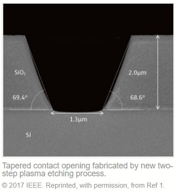
Current methods for creating channels, called vias, with tapered sidewalls in MEMS at scales of five microns or less, are not dependable. The etching method, with sidewall polymerization, is not suitable as the width at the bottom of the vias shrink considerably. Another method, involving the transfer of a photoresist profile into an etched layer, limits the maximal depth of vias due to excessive loss of the photoresist mask resulting in unacceptably rough sidewalls.
To overcome these restrictions, the researchers developed a two-step plasma etching process. This combines firstly photoresist tapering, which modifies the photoresist from a vertical to a tapered profile, and then an oxide etching with sidewall polymerization with better selectivity to photoresist. This produces vias with minimal dimensions down to 1.5 microns, and smooth sidewalls with angles of around 70 degrees.
“We combined two effects which are usually harmful during the etching process — accelerated corner sputtering and sidewall polymerization,” explains Bliznetsov.
Combining these processes into a two-step method achieves greater control over the etching process and produces micron-sized vias with smooth, tapered walls. And by minimizing the sidewall angle of the vias, it is possible to fabricate devices that can be better protected and have more reliable metal contacts, greatly improving their performance.
“Precise control of sidewall angle has use in many applications, and we are now planning to fabricate functional magnetic memory cells, which require pillars of magnetic material with sidewalls having a specific angle,” says Bliznetsov.
Share on:


Testimonial
"In a year when every marketing dollar mattered, I chose to keep I-Connect007 in our 2025 plan. Their commitment to high-quality, insightful content aligns with Koh Young’s values and helps readers navigate a changing industry. "
Brent Fischthal - Koh YoungSuggested Items
Closing the Loop on PCB Etching Waste
09/09/2025 | Shawn Stone, IECAs the PCB industry continues its push toward greener, more cost-efficient operations, Sigma Engineering’s Mecer System offers a comprehensive solution to two of the industry’s most persistent pain points: etchant consumption and rinse water waste. Designed as a modular, fully automated platform, the Mecer System regenerates spent copper etchants—both alkaline and acidic—and simultaneously recycles rinse water, transforming a traditionally linear chemical process into a closed-loop system.
The Chemical Connection: Through-glass Vias in Glass Substrates
06/24/2025 | Don Ball -- Column: The Chemical ConnectionThis month’s theme is vias and how best to ensure via quality and reliability. I don’t have much expertise in this process area or much to contribute that most of you don’t already know. However, I’ve recently become peripherally involved in a via technology that may be of more than academic interest to some of us. It entails putting vias in a material not usually associated with PCB manufacturing: through-glass vias (TGVs) in glass substrates.
In Pursuit of Perfection: Defect Reduction—May 2025 PCB007 Magazine Now Available
05/15/2025 | I-Connect007 Editorial TeamFor bare PCB board fabrication, defect reduction is a critical aspect of a company's bottom line profitability. In the May 2025 issue of PCB007 Magazine, we examine the imaging, etching, and plating processes, as well as product traceability on the shop floor, providing information and insight into how you can reduce your defects and increase yields.
DuPont to Showcase Advanced Semiconductor Wet Etching Innovations at the Surface Preparation and Cleaning Conference
05/13/2025 | DuPontDuPont announced that it will present its latest developments in semiconductor wet etching technologies at the upcoming Surface Preparation and Cleaning Conference (SPCC) in Chandler, Arizona, beginning May 20.
The Chemical Connection: Common Misconceptions in Wet Processing
04/28/2025 | Don Ball -- Column: The Chemical ConnectionInitially, I thought an April Fool’s column would be fun this month. I could highlight some of the crazier ideas and misconceptions I’ve witnessed over the years from potential customers and we could all have a good laugh. For example, there was a first-time buyer of a ferric chloride etcher (with no regeneration system) who was astonished to learn that he had to put fresh etchant in the system occasionally to maintain production.