


 Trouble in Your Tank: Implementing Direct Metallization in Advanced Substrate Packaging
 It’s Only Common Sense: Storytelling That Sells—Stop Pitching, Start Painting Pictures
 The Right Approach: Get Ready for ISO 9001 Version 6


Tiny Droplets for Big Color Impact
March 26, 2018 | A*STAREstimated reading time: 2 minutes
Color prints produced on contemporary printers have a resolution of a few thousand dots per inch (dpi), but an alternative strategy that harnesses the power of nanotechnology can improve this resolution by an order of magnitude.
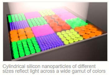
Depositing ink droplets on a surface to create color pictures is a centuries-old technology. A*STAR researchers are now testing a new method, which uses an array of nanostructures that reflect light of the desired color. As these structures, or pixels, are much smaller than ink drops, a resolution of up to 100,000 dpi could, in principle, be achieved.
Nanostructures influence light through so-called optical resonances. In the case of metals, these optical resonances are due to the excitation of plasmons – light strongly couples to spatially-confined electrons on the surface, and is either absorbed or reflected depending on its wavelength. The peak reflectivity wavelength, and thus the apparent color of the pixel, is tunable by changing the dimensions of the nanostructures.
Plasmonic materials are often noble metals, such as gold and silver, or aluminum. But these materials are constrained by price, spectrum coverage, or the low purity of the color they reflect.
Ramón Paniagua-Domínguez from the A*STAR Data Storage Institute and co-workers investigate semiconductor nanostructures made of silicon. They measure the optical properties of an array of discs with diameters ranging from 50 to 250 nanometers under illumination conditions suited for a practical implementation.
“We compared the quality of colors generated by silicon particles with those from silver and aluminum plasmonic particles,” says Paniagua-Domínguez. “We showed that the colors obtained are of far better quality in terms of hue, gamut and intensity.”
The improvement is because the colors from silicon do not stem from plasmonic resonances as they do in the noble metals, but rather from geometrical resonances that originate from bound electrons. Consequently, silicon is less affected by absorption losses than silver or aluminum and so can produce a sharper reflectance spectrum, meaning a better color purity.
The technology for fabricating silicon nanostructures is well developed due to its broad adoption in the manufacture of electronics. Thanks to this they were able to reproduce masterpieces such as Edvard Munch’s The Scream in an area smaller than one square-millimeter.
“Our focus is on expanding the color gamut to go beyond the standard widely adopted in the display industry,” says Paniagua-Domínguez. “We will also explore mechanisms to actively control the resonances, and therefore the color, of the particles, to bring this technology closer to application in ultra-high-definition displays.”
Share on:


Testimonial
"Our marketing partnership with I-Connect007 is already delivering. Just a day after our press release went live, we received a direct inquiry about our updated products!"
Rachael Temple - AlltematedSuggested Items
Advint Incorporated Brings Artificial Intelligence to Electroplating Training
09/11/2025 | Advint IncorporatedAdvint Incorporated is introducing a new dimension to its electroplating training programs: the integration of Artificial Intelligence (AI). This initiative reflects the company’s commitment to providing PCB fabricators and manufacturers in the USA and Canada with training that is practical, forward-looking, and directly relevant to today’s production challenges.
The Signal Integrity Issue: Design007 Magazine September 2025
09/09/2025 | I-Connect007 Editorial TeamAs the saying goes, “If you don’t have signal integrity problems now, you will eventually.” This month, our experts share a variety of design techniques that can help PCB designers and design engineers achieve signal integrity.
Semiconductors Get Magnetic Boost with New Method from UCLA Researchers
07/31/2025 | UCLA NewsroomA new method for combining magnetic elements with semiconductors — which are vital materials for computers and other electronic devices — was unveiled by a research team led by the California NanoSystems Institute at UCLA.
SMT Perspectives and Prospects: Warren Buffett’s Perpetual Wisdom, Part 1
07/29/2025 | Dr. Jennie Hwang -- Column: SMT Perspectives and ProspectsOver the years, I have cherished the lessons by Warren Buffett and Charlie Munger at the Berkshire Hathaway annual shareholders meeting in Omaha, Nebraska. This year, I was among the more than 40,000 who attended the May 3 meeting. Millions more from around the world, including from the UK, Germany, Japan, China, Panama, and Guatemala, tuned in remotely and via CNBC’s livestream.
Mesa West, Advanced West Announce Strategic Partnership
06/15/2025 | I-Connect007Mesa West is proud to announce that they have officially joined forces with Advanced West. This strategic partnership brings together two industry leaders, uniting strengths to better serve customers through enhanced capabilities, expanded offerings, and continued commitment to quality.