


 Trouble in Your Tank: Implementing Direct Metallization in Advanced Substrate Packaging
 It’s Only Common Sense: Storytelling That Sells—Stop Pitching, Start Painting Pictures
 The Right Approach: Get Ready for ISO 9001 Version 6


Tuning In to Magnetic Ink
April 2, 2018 | KAUSTEstimated reading time: 1 minute
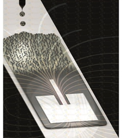
Inkjet printing technology can be used to produce radio frequency devices, such as antennas, that can be magnetically reconfigured on demand. This discovery by a team from KAUST boosts prospects for inexpensive electronics that work worldwide by tuning in to multiple cellular bands and standards.
A typical cellphone antenna is made by depositing metallic patterns onto insulating silicon or glass wafers. These miniature aerials have excellent reliability, but only operate at fixed frequency bands. To fabricate devices that can adapt to different wireless settings, researchers are increasingly turning to magnets. Replacing an insulating wafer with a magnetic one, for instance, can achieve frequency tuning that can cover mega- to gigahertz ranges.
Instead of the complex, multilayered ceramics currently used as magnetic substrates, Mohammad Vaseem, Atif Shamim and colleagues investigated an approach based on printable electronics—a technology that replaces the dye-filled fluids found in consumer printers with special inks containing substances, such as metallic nanoparticles, and then custom-prints device patterns with relative ease and high speeds.
“If magnetic substrates can be printed, we can achieve huge cost savings and add new functionalities,” says Shamim. “There are a number of other metrics that can be optimized, such as thickness, that are impossible with fixed substrates.”
By injecting iron-based reagents into a hot acetic acid solution, the researchers synthesized magnetic iron-oxide nanoparticles that dispersed into deionized water to form an ink. Subsequent printing tests showed immediate promise: when deposited as a thin film on a glass substrate, the new magnetic substrate could act as an energy-storing inductor device with an adjustable capacity of over 20 percent.
Printing the magnetic ink thicker than a few nanometers, however, proved impossible due to its natural brittleness. To strengthen the ink, the team modified the nanoparticles’ surfaces with hydrocarbon chains to help the tiny magnets mix evenly into an epoxy resin known as SU-8. The resulting paste was screen-printed and UV-cured into free-standing magnetic sheets of a few millimeters in thickness.
The innovative, fully printed magnetic wafer displayed promising antenna tuning of over 10 percent—a figure the team aims to improve by perfecting their printing recipes.
“The surprise was that we got antennas with a good tuning range, even though we mixed in 50 percent SU-8,” notes Shamim. “This means we could extend this tuning range further by adjusting this ratio and also move to more sophisticated roll to roll processes that print at meters per minute.”
Share on:


Testimonial
"Advertising in PCB007 Magazine has been a great way to showcase our bare board testers to the right audience. The I-Connect007 team makes the process smooth and professional. We’re proud to be featured in such a trusted publication."
Klaus Koziol - atgSuggested Items
Printed Electronics Market Size to Top $83.77 Billion by 2034 Driven by IoT Adoption and Flexible Device Demand
09/11/2025 | Globe NewswireThe printed electronics market size has been calculated at U$19,920 million in 2025 and is expected to grow from $23,58 million in 2026 to approximately $83,770 million by 2034.
Electroninks Acquires Complete UTDots Advanced Materials Nanoinks Portfolio and IP
05/19/2025 | ElectroninksElectroninks, the leader in metal organic decomposition (MOD) inks for additive manufacturing and advanced semiconductor packaging, announced it has officially completed its full acquisition of UTDots products and IP into its portfolio, further expanding its offerings in digital printing for high-performance applications.
Happy’s Tech Talk #38: Novel Metallization for UHDI
05/07/2025 | Happy Holden -- Column: Happy’s Tech TalkI have been involved in high-density electronics substrates since 1970 when I joined Hewlett-Packard’s RF semiconductor group after college. Figure 1 shows the difference between trace/space lithography for substrates and silicon starting in 1970. My projects involved sapphire circuits for RF devices, but the figure displays the state of PCBs and integrated CMOS circuits and their packaging, not discreet RF devices. Even then, semiconductors were 50X higher density.
Real Time with... IPC APEX EXPO 2025: Emerging Trends in Design and Technology
04/16/2025 | Real Time with...IPC APEX EXPOAndy Shaughnessy speaks with IPC design instructor Kris Moyer to discuss emerging design trends. They cover UHDI technology, 3D printing, and optical data transmission, emphasizing the importance of a skilled workforce. The role of AI in design is highlighted, along with the need for understanding physics and mechanics as designs become more complex. The conversation concludes with a focus on enhancing math skills for better signal integrity.
Real Time with... IPC APEX EXPO 2025: Transition Automation Focusing on Security Coatings and Squeegee Technology
04/16/2025 | Real Time with...IPC APEX EXPOMark Curtin, President of Transition Automation, gives an update on recent innovations at his company. He highlights a record sales month and their new focus on security coatings to fight counterfeiting. Mark explains the engineering behind their durable squeegees, the importance of maintenance, and the value of considering overall costs over just price.