


 American Made Advocacy: Smart Policies Can Ensure AI Data Centers Are Secure
 Beyond the Board: Early Engagement Means Faster Prototyping for Defense Programs
 Defense Speak Interpreted: The Autonomous Plane Battle—Skyborg Vs. Loyal Wingman


Innovative Detectors Quickly Pinpoint Radiation Source
April 3, 2018 | Los Alamos National LaboratoryEstimated reading time: 1 minute
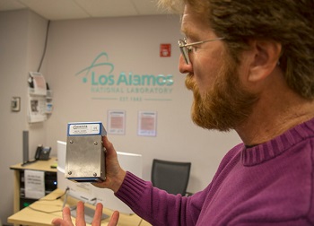
Innovative “lighthouse” detectors that use a sweeping beam to quickly pinpoint a radiation source in seconds are reducing radiation exposure for workers and opening up new areas for robotic monitoring to avoid potential hazards.
“It’s easier to find a needle in a haystack if the haystack is small,” said Jonathan Dowell, a Los Alamos scientist and inventor of the detector. He was referring to the detectors’ ability to hone in on an area while eliminating background noise or naturally occurring radiation.
On the detectors, directional sensors similar to a beam atop a lighthouse scan through a narrow angle looking for radiation. The Laboratory uses the detectors aboard HAZMAT robots for emergency response, as well as to conduct geologic surveys.
“The more we can reduce radiation exposure, the better it is for the people doing the work,” said Dowell. “Using a robot or automated machines can help.”
The small radiation detectors, patented by Los Alamos National Laboratory and commercialized by industrial partner Quaesta Instruments, are easy to carry and deploy. “We’ve taken what used to be the size of a baseball bat and miniaturized it to the size of a jar of peanut butter,” said Dowell.
In a test later this year, numerous detectors will be deployed using a robot to survey radioactive materials at the Trinity Site. In addition to the historical significance of measuring minute traces of such materials, the survey will also demonstrate the ability to test large areas in a short time while eliminating the need for workers to enter a site. “A detector will be deployed on a robot’s arm like a doctor would hold a stethoscope to your chest,” said Dowell. “It will reach down into nooks and crannies.”
The detectors can be used in various applications including locating contaminants at waste sites, conducting inventory, tracking the movement of radioactive materials for national security purposes, and verifying that areas are free of radioactive sources.
Industries that can benefit from the technology include universities and hospitals.
Share on:


Testimonial
"The I-Connect007 team is outstanding—kind, responsive, and a true marketing partner. Their design team created fresh, eye-catching ads, and their editorial support polished our content to let our brand shine. Thank you all! "
Sweeney Ng - CEE PCBSuggested Items
Sealed for Survival: Potting Electronics for the Toughest Environments
10/29/2025 | Beth Massey, MacDermid Alpha Electronics SolutionsElectronics deployed in harsh conditions face relentless threats from vibration, impact, chemical contaminants, airborne pollutants, and moisture, conditions that can quickly lead to failure without robust protection. Potting, the process of encapsulating electronics in a protective polymer, is a widely used strategy to safeguard devices from both environmental and mechanical hazards.
Driving Innovation: Mechanical and Optical Processes During Rigid-flex Production
10/28/2025 | Kurt Palmer -- Column: Driving InnovationRigid-flex printed circuit boards are a highly effective solution for placing complex circuitry in tight, three-dimensional spaces. They are now indispensable across a range of industries, from medical devices and aerospace to advanced consumer electronics, helping designers make the most efficient use of available space. However, their unique construction—combining rigid and flexible materials—presents a fundamental challenge for PCB manufacturers.
SMTAI 2025 Review: Reflecting on a Pragmatic and Forward-looking Industry
10/27/2025 | Marcy LaRont, I-Connect007Leaving the show floor on the final afternoon of SMTA International last week in Rosemont, Illinois, it was clear that the show remains a grounded, technically driven event that delivers a solid program, good networking, and an easy space to commune with industry colleagues and meet with customers.
ITW EAE Despatch Ovens Now Support ASTM 5423 Testing
10/15/2025 | ITW EAEAs the demand for high-performance electrical insulation materials continues to grow—driven by the rapid expansion of electric vehicles (EVs) and energy storage systems—thermal processing has become a critical step in material development.
Beyond Thermal Conductivity: Exploring Polymer-based TIM Strategies for High-power-density Electronics
10/13/2025 | Padmanabha Shakthivelu and Nico Bruijnis, MacDermid Alpha Electronics SolutionsAs power density and thermal loads continue to increase, effective thermal management becomes increasingly important. Rapid and efficient heat transfer from power semiconductor chip packages is essential for achieving optimal performance and ensuring long-term reliability of temperature-sensitive components. This is particularly crucial in power systems that support advanced applications such as green energy generation, electric vehicles, aerospace, and defense, along with high-speed computing for data centers and artificial intelligence (AI).