


 Knocking Down the Bone Pile: Revamp Your Components with BGA Reballing
 Global Sourcing Spotlight: Balancing Speed and Flexibility Without Sacrificing Control
 SMT Perspectives & Prospects: Artificial Intelligence Part 6: Data Module 1


Stencil Printing Techniques for Challenging Heterogeneous Assembly Applications
April 16, 2018 | Mark Whitmore and Jeff Schake, ASM Assembly SystemsEstimated reading time: 3 minutes
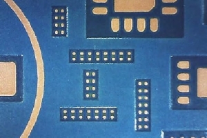
A new generation of near microscopic size SMT chip capacitors has appeared in the market, known as either 0201 (metric dimension label) or 008004 (imperial dimension label). Assembly results using these components is so far largely obscured from publication and highly proprietary. All aspects of the assembly process are expected to be challenged to accommodate the extreme level of miniaturization embodied in this device. The objective of this research is to investigate and characterize the stencil printing process for compatibility with M0201 (metric 0201) capacitor assembly. Effects of circuit board quality, stencil thickness, and stencil nano-coating are the primary experiment variables reported against solder paste volume transfer efficiency and raw-volume print distribution.
Figure 1: M0201 capacitor dimensions and tolerances.
M0201
The designation M0201 implies a case size length of 0.2mm and width of 0.1mm, when in fact these are produced at nominal dimensions of 0.25mm x 0.125mm (Figure 1).
In a footprint-area comparison, the M0201 covers only 39% of a M0402 (imperial 01005) chip component. M0201 capacitors were first commercially available for volume prototype assembly testing in 2014. Resistor M0201 passives are not yet known to be offered.
PCB land design options for M0201 are shown in Figure 2 as prescribed by the component manufacturer. The smallest pad size is 125μm x 70μm, which approximately matches the metal end terminal footprint. The largest pad size nearly doubles the smallest pad size area at 145μm x 120μm.
The pad design of our preference is shown in Figure 3, which is at the top limit of the suggested pad size range. The motivation for using such sizeable pad dimensions include:
Figure 2: M0201 vendor pad size recommendations.
Over-etched Cu is expected to be problematic at this dimensional scale. Using the largest Cu pad design should at least help to improve PCB manufacturability.
Typically, the stencil aperture size mimics pad the dimensions. The largest pad area offers to ease aperture area ratios and permits potentially improved print volume control.
Prerequisite Solder Volume
The determination of a suitable stencil aperture capacity requires prerequisite knowledge of the appropriate reflowed solder joint form. The IPC-A-601E standard was consulted as an appropriate reference to determine this. Figure 4 illustrates the model used to establish the structure of an acceptable M0201 solder joint of minimum volume. Author judgment prevailed for dimensions not explicitly provided in the 601E standard. The determination of this smallest solder volume is helpful in establishing a stencil design and for evaluating print performance against solder paste inspection (SPI) data.
Figure 3: Selected M0201 pad design for drint study
The geometry of the soldered terminations with minimum solder volume have been simplified as triangles at the sides (V1, V2) and end of the terminal contact (V3) while the largest volume contributor to the solder joint is the rectangular area underneath it (V4). The solder thickness dimension G contributes substantially to the overall solder joint volume. As the objective here is to determine a minimum solder volume, our interpretation of the 601E standard does not require the pad to be fully wetted to form an acceptable solder joint shape. An acceptable ratio of solder paste to metal by volume is 2:1. From this it is found that each chip component termination should require at least 0.48 nanoliters (1nl = 1,000,000μm3) of printed solder paste volume to form an acceptable reflowed solder joint. Note this amount scales to the pad dimensions selected (i.e., smaller pads will not require as much solder paste to comply).
Figure 4: Minimum solder volume termination model.
The printing stencil must be designed with aperture opening dimensions that will allow solder paste transfer accomplishing at least 0.48nl per pad. The difficulty in achieving this relates to practical restrictions on stencil thickness. For the products likely to see earliest implementation of M0201s, common stencil thickness used today is 100μm. The inclusion of M0201 will compel the use of even thinner stencil foils to reduce the risk of producing insufficient volume paste deposits attributed to clogged apertures. It is well documented that print transfer efficiency (TE) of solder paste scales proportionally to stencil aperture area ratio. Area ratio (AR) is defined as the aperture opening area divided by the aperture wall area.
AR values reducing further away from 0.6 will escalate average paste transfer loss while also increasing scatter in printed deposit size and shape.
To read the full article, which appeared in the March 2018 issue of SMT007 Magazine, click here.
Share on:


Testimonial
"Our marketing partnership with I-Connect007 is already delivering. Just a day after our press release went live, we received a direct inquiry about our updated products!"
Rachael Temple - AlltematedSuggested Items
Rehm Wins Mexico Technology Award for CondensoXLine with Formic Acid
10/17/2025 | Rehm Thermal SystemsModern electronics manufacturing requires technologies with high reliability. By using formic acid in convection, condensation, and contact soldering, Rehm Thermal Systems’ equipment ensures reliable, void-free solder joints — even when using flux-free solder pastes.
Indium Experts to Deliver Technical Presentations at SMTA International
10/14/2025 | Indium CorporationAs one of the leading materials providers to the power electronics assembly industry, Indium Corporation experts will share their technical insight on a wide range of innovative solder solutions at SMTA International (SMTAI), to be held October 19-23 in Rosemont, Illinois.
Knocking Down the Bone Pile: Revamp Your Components with BGA Reballing
10/14/2025 | Nash Bell -- Column: Knocking Down the Bone PileBall grid array (BGA) components evolved from pin grid array (PGA) devices, carrying over many of the same electrical benefits while introducing a more compact and efficient interconnect format. Instead of discrete leads, BGAs rely on solder balls on the underside of the package to connect to the PCB. In some advanced designs, solder balls are on both the PCB and the BGA package. In stacked configurations, such as package-on-package (PoP), these solder balls also interconnect multiple packages, enabling higher functionality in a smaller footprint.
Indium to Showcase High-Reliability Solder and Flux-Cored Wire Solutions at SMTA International
10/09/2025 | Indium CorporationAs one of the leading materials providers in the electronics industry, Indium Corporation® will feature its innovative, high-reliability solder and flux-cored wire products at SMTA International (SMTAI), to be held October 19-23 in Rosemont, Illinois.
‘Create your Connections’ – Rehm at productronica 2025 in Munich
10/08/2025 | Rehm Thermal SystemsThe electronics industry is undergoing dynamic transformation: smart production lines, sustainability, artificial intelligence, and sensor technologies dominate current discussions.