


 Trouble in Your Tank: Implementing Direct Metallization in Advanced Substrate Packaging
 It’s Only Common Sense: Storytelling That Sells—Stop Pitching, Start Painting Pictures
 The Right Approach: Get Ready for ISO 9001 Version 6


Surface Engineering Gets the Red Light
April 23, 2018 | KAUSTEstimated reading time: 2 minutes
A method for chemically stabilizing optical nanocrystals, without degrading their electrical properties, has been developed by scientists at KAUST.
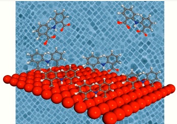
Image caption: Passivating the surface of perovskite nanocrystals with IDA molecules improves their stability and their optical and electrical properties, making them useful for optoelectronic devices.
Halide perovskites are in an exciting class of materials for optoelectronics and photovoltaics. These materials efficiently absorb visible light, possess long charge-carrier diffusion lengths and are easy and cheap to produce. The performance of optical devices can also be improved by incorporating nanometer-scale particles, which have far superior light-emitting and -absorbing properties than the bulk material from which they are derived. So it is unsurprising that scientists are keen to combine these two approaches. The challenge is that tiny perovskite particles aren’t always chemically stable, and their atomic crystal structure is difficult to control.
Attaching molecules, referred to as ligands, can stabilize a nanocrystal. But this so-called passivation can form an electrically insulating shell around the particle that inhibits their effectiveness in electronic devices.
Now, Osman Bakr’s group, and co-workers from KAUST and ShanghaiTech University, has created halide perovskite nanocrystals made from cesium-lead-iodide passivated by 2,2′-iminodibenzoic acid (IDA) ligands. They show that this provides the necessary chemical stability while remaining useful for optoelectronics. And the passivation was simple: just adding IDA powder into the nanocrystal solution and using a centrifuge to remove any excess.
The team chose IDA because it is a bidentate ligand, meaning that it bonds to the nanocrystal at two sites. “The conventional ligands used in these applications, such as oleic acid, are dynamic on the surface of the perovskite nanocrystals and easily come loose,” says Jun Pan, the first author on the paper. “That’s why we apply a double carboxylic group to strongly bind on the surface, which also stabilizes the perovskite crystal phase at room temperature.”
Pan and his team compared the optical properties of both the passivated and unpassivated samples and observed that the treatment improved the photoluminescent quantum yield—a measure of how many photons are emitted for every photon absorbed—from 80 percent to over 95 percent. And while the intensity of light emitted from the unpassivated nanocrystals had dropped significantly five days later, the IDA-treated samples were still emitting light at 90 percent of their initial level 15 days later.
Passivating the surface of perovskite nanocrystals with IDA molecules improves their stability and their optical and electrical properties, making them useful for optoelectronic devices.
The team demonstrated that their stabilized halide perovskite nanocrystals were suitable for optoelectronic applications by using them to build light-emitting diodes. The red-light generating devices again outperformed the unpassivated control device in terms of maximum luminance and luminous power efficiency.
“The next step is to realize more stable perovskite structures and to create an LED with performance above 10 percent based on perovskite nanocrystals,” says Pan.
Share on:


Testimonial
"Advertising in PCB007 Magazine has been a great way to showcase our bare board testers to the right audience. The I-Connect007 team makes the process smooth and professional. We’re proud to be featured in such a trusted publication."
Klaus Koziol - atgSuggested Items
Driving Innovation: Depth Routing Processes—Achieving Unparalleled Precision in Complex PCBs
09/08/2025 | Kurt Palmer -- Column: Driving InnovationIn PCB manufacturing, the demand for increasingly complex and miniaturized designs continually pushes the boundaries of traditional fabrication methods, including depth routing. Success in these applications demands not only on robust machinery but also sophisticated control functions. PCB manufacturers rely on advanced machine features and process methodologies to meet their precise depth routing goals. Here, I’ll explore some crucial functions that empower manufacturers to master complex depth routing challenges.
Polar Instruments Announces Additive Transmission Line Support for Si9000e
08/20/2025 | Polar InstrumentsTransmission lines embedded into the PCB surface are a feature of UHDI constructions. The 2025 fall release of Polar's Si9000e PCB impedance & insertion loss transmission line field solver incorporates eight new single ended, differential and coplanar transmission line structures.
Henniker Plasma Launches Stratus Turnkey Plasma Manufacturing Cell
08/13/2025 | Henniker PlasmaHenniker Plasma, a leading manufacturer of plasma treatment systems, proudly announces the launch of its Stratus Plasma Manufacturing Cell range — a fully integrated, turnkey solution that combines advanced atmospheric plasma surface treatment with robotic automation.
Trouble in Your Tank: Metallizing Flexible Circuit Materials—Mitigating Deposit Stress
08/04/2025 | Michael Carano -- Column: Trouble in Your TankMetallizing materials, such as polyimide used for flexible circuitry and high-reliability multilayer printed wiring boards, provide a significant challenge for process engineers. Conventional electroless copper systems often require pre-treatments with hazardous chemicals or have a small process window to achieve uniform coverage without blistering. It all boils down to enhancing the adhesion of the thin film of electroless copper to these smooth surfaces.
Designers Notebook: Basic PCB Planning Criteria—Establishing Design Constraints
07/22/2025 | Vern Solberg -- Column: Designer's NotebookPrinted circuit board development flows more smoothly when all critical issues are predefined and understood from the start. As a basic planning strategy, the designer must first consider the product performance criteria, then determine the specific industry standards or specifications that the product must meet. Planning also includes a review of all significant issues that may affect the product’s manufacture, performance, reliability, overall quality, and safety.