


 Trouble in Your Tank: Implementing Direct Metallization in Advanced Substrate Packaging
 It’s Only Common Sense: Storytelling That Sells—Stop Pitching, Start Painting Pictures
 The Right Approach: Get Ready for ISO 9001 Version 6


Why Perovskite Solar Cells Are So Efficient
April 25, 2018 | KITEstimated reading time: 2 minutes
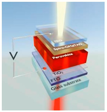
Solar cells with efficiencies above 20% and produced at low costs—perovskites make this possible. Now, researchers of Karlsruhe Institute of Technology (KIT) have gained fundamental insight into the function of perovskite solar cells. They found that bound states of electron-hole pairs can form during the absorption of light. Still, these pairs can be separated easily for current to flow. In addition, they enhance absorption. Perovskites are among the most promising materials for solar cells: When using them, the high efficiency can be combined with low-cost production. Photovoltaics research focuses on halide perovskites that contain both organic and inorganic compounds and, hence, are considered hybrid semiconductors. “In less than one decade, these perovskites underwent an outstanding development. Meanwhile, perovskite solar cells convert more than 20% of the incident light directly into usable current,” says photovoltaics expert Dr. Michael Hetterich of KIT, who coordinates collaboration between KIT and the Center for Solar Energy and Hydrogen Research Baden-Württemberg (ZSW). The vast potential of perovskites is also obvious from tandem solar cells that combine a semitransparent perovskite top cell with a silicon or copper-indium-gallium-diselenide (CIGS) bottom cell. This allows for an optimal use of the solar spectrum.
Current research challenges consist in enhancing the long-term stability of perovskite solar cells and replacing the lead they contain by environmentally more compatible elements. This requires deep insight into the structure and function of the perovskite layers. Researchers of the Institute of Applied Physics and the Light Technology Institute of KIT as well as of ZSW and Ludwig-Maximilians-Universität München study the function of thin-layer tandem solar cells based on perovskites under the CISOVSKIT (development of highly efficient hybrid solar cells from CIGS and perovskite materials) project funded by the Federal Ministry of Education and Research (BMBF). And they obtained new findings relating to the physical nature of the optical transitions.
Optical transitions are changes of the energy state of electrons in a material by emission (release) or absorption (uptake) of photons, i.e. light particles. In his doctoral thesis, Fabian Ruf, who works in the group of Professor Heinz Kalt, KIT, points out that the fundamental optical transition in solar cells with a methyl ammonium lead iodide absorber, the classical halide perovskite, is of excitonic nature. This means that excitons may form in the solar cells after the absorption of light particles. Excitons are bound electron-hole pairs that largely determine the optoelectronic properties. Binding energy of the excitons has to be overcome in order to obtain free charge carriers and to make the current flow.
By means of temperature-dependent electroabsorption spectroscopy, Fabian Ruf studied semitransparent solar cells with methyl ammonium lead iodide absorbers produced by Moritz Schultes of ZSW by a wet chemistry method. The results allow conclusions to be drawn with respect to excitonic transitions over the complete temperature range studied, from 10 Kelvin (-263°C) to room temperature. Depending on the perovskite crystal structure that changes with changing temperature, the exciton binding energy amounts to about 26 and 19 millielectronvolts, respectively. “Hence, the binding energy is small enough to ensure sufficient thermal separation of charge carriers at room temperature,” Michael Hetterich explains. “In addition, the excitonic effects enhance absorption. Both effects together enable efficient operation of the perovskite solar cell.”
Share on:


Testimonial
"Advertising in PCB007 Magazine has been a great way to showcase our bare board testers to the right audience. The I-Connect007 team makes the process smooth and professional. We’re proud to be featured in such a trusted publication."
Klaus Koziol - atgSuggested Items
Trouble in Your Tank: Implementing Direct Metallization in Advanced Substrate Packaging
09/15/2025 | Michael Carano -- Column: Trouble in Your TankDirect metallization systems based on conductive graphite are gaining popularity throughout the world. The environmental and productivity gains achievable with this process are outstanding. Direct metallization reduces the costs of compliance, waste treatment, and legal issues related to chemical exposure. A graphite-based direct plate system has been devised to address these needs.
Closing the Loop on PCB Etching Waste
09/09/2025 | Shawn Stone, IECAs the PCB industry continues its push toward greener, more cost-efficient operations, Sigma Engineering’s Mecer System offers a comprehensive solution to two of the industry’s most persistent pain points: etchant consumption and rinse water waste. Designed as a modular, fully automated platform, the Mecer System regenerates spent copper etchants—both alkaline and acidic—and simultaneously recycles rinse water, transforming a traditionally linear chemical process into a closed-loop system.
Driving Innovation: Depth Routing Processes—Achieving Unparalleled Precision in Complex PCBs
09/08/2025 | Kurt Palmer -- Column: Driving InnovationIn PCB manufacturing, the demand for increasingly complex and miniaturized designs continually pushes the boundaries of traditional fabrication methods, including depth routing. Success in these applications demands not only on robust machinery but also sophisticated control functions. PCB manufacturers rely on advanced machine features and process methodologies to meet their precise depth routing goals. Here, I’ll explore some crucial functions that empower manufacturers to master complex depth routing challenges.
Trouble in Your Tank: Minimizing Small-via Defects for High-reliability PCBs
08/27/2025 | Michael Carano -- Column: Trouble in Your TankTo quote the comedian Stephen Wright, “If at first you don’t succeed, then skydiving is not for you.” That can be the battle cry when you find that only small-diameter vias are exhibiting voids. Why are small holes more prone to voids than larger vias when processed through electroless copper? There are several reasons.
The Government Circuit: Navigating New Trade Headwinds and New Partnerships
08/25/2025 | Chris Mitchell -- Column: The Government CircuitAs global trade winds continue to howl, the electronics manufacturing industry finds itself at a critical juncture. After months of warnings, the U.S. Government has implemented a broad array of tariff increases, with fresh duties hitting copper-based products, semiconductors, and imports from many nations. On the positive side, tentative trade agreements with Europe, China, Japan, and other nations are providing at least some clarity and counterbalance.