


 Trouble in Your Tank: Implementing Direct Metallization in Advanced Substrate Packaging
 It’s Only Common Sense: Storytelling That Sells—Stop Pitching, Start Painting Pictures
 The Right Approach: Get Ready for ISO 9001 Version 6


Infrared Spectrometer on a Chip
May 9, 2018 | Agência FAPESPEstimated reading time: 2 minutes
Fourier-transform infrared (FTIR) spectrometers, among the most frequently used research tools to identify and analyze chemicals, are too large to be used in the field to detect compounds.
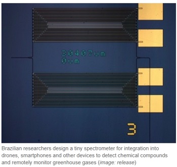
Several attempts have been made to develop miniaturized FTIR spectrometers for integration into drones to monitor greenhouse gases remotely, for example, or for integration into smartphones and other devices. However, current miniaturized devices are costly to produce and therefore cannot be widely used.
Scientists at the University of Campinas’s Device Research Laboratory (LPD-UNICAMP) in Brazil, collaborating with colleagues at the University of California San Diego in the United States, have overcome these constraints by developing an FTIR spectrometer based on silicon photonics, the technology currently used to produce chips for computers, smartphones and other electronic devices.
Resulting from Mário César Mendes Machado de Souza’s PhD research and a research internship abroad, supported by scholarships from FAPESP and supervised by Professor Newton Frateschi, the new spectrometer is described in an article published in Nature Communications. Souza is the article’s lead author and thought up the project.
“Silicon photonics offers a platform for the fabrication of affordable high-performance miniaturized spectrometers,” he told Agência FAPESP.
According to Souza, FTIR spectroscopy identifies chemicals using an infrared light source to measure absorption. A sample is exposed to different wavelengths of infrared light, and the spectrometer measures which wavelengths are absorbed. The computer takes these raw absorption data and conducts a mathematical process known as the Fourier transform to generate an absorbance pattern or spectrum, which is compared to a library of spectra for chemical compounds to find a match.
Various projects have appeared in recent years to develop an FTIR spectrometer based on integrated photonics, which uses light especially in the infrared spectrum, but progress had so far been scant owing to several technical challenges, Souza explained.
One of these challenges is the highly dispersive profile of silicon waveguides, meaning that each wavelength travels at a different speed in this material and hence has a different refractive index.
The refractive indices of optical waveguides in silicon can be “tuned” by means of the thermo-optical effect, which involves passing a current over the waveguide in order to heat it. Because the device has to be operated at high temperatures in order to achieve high resolution, this technique becomes non-linear in the sense that changes in temperature correlate with disproportionate changes in the refractive index.
“In practice, what happens when a thermo-optical effect is applied to a silicon-based infrared spectrometer with integrated photonics is that the Fourier transform mathematical operations used to convert the radiation spectrum data collected produce completely wrong results,” Souza explained.
The researchers succeeded in overcoming these challenges by creating a laser calibration method to quantify and correct the distortions caused by silicon waveguide dispersion and non-linearity. As a proof of concept, they developed a 1 mm² FTIR spectrometer chip based on standard silicon photonics fabrication procedures.
The chip was tested in the laboratory, producing a broadband spectrum with a resolution of 0.38 terahertz (THz), which is comparable with the resolution of commercially available portable spectrometers that operate in the same wavelength range, according to the researchers.
“The device we developed is far from optimized but still achieves resolutions comparable with those of the portable free-space optics-based spectrometers available in the market today,” Souza said.
The researchers now plan to engineer a device that is totally functional and integrated with photodetectors, light sources and optical fibers.
“Our goal is to integrate the light source and the spectrometer’s detector into the same platform,” Souza said.
Share on:


Testimonial
"We’re proud to call I-Connect007 a trusted partner. Their innovative approach and industry insight made our podcast collaboration a success by connecting us with the right audience and delivering real results."
Julia McCaffrey - NCAB GroupSuggested Items
Rules of Thumb: Design007 Magazine, November 2024
11/11/2024 | I-Connect007 Editorial TeamRules of thumb are everywhere, but there may be hundreds of rules of thumb for PCB design. They’re built on design formulas, fabricators’ limitations, and tribal knowledge. And unfortunately, some longtime rules of thumb should be avoided at all costs. How do we separate the wheat from the chaff, so to speak?
Connect the Dots: Best Practices for Prototyping
09/21/2023 | Matt Stevenson -- Column: Connect the DotsPCB prototyping is a critical juncture during an electronic device’s journey from concept to reality. Regardless of a project’s complexity, the process of transforming a design into a working board is often enlightening in terms of how a design can be improved before a PCB is ready for full production.
The Drive Toward UHDI and Substrates
09/20/2023 | I-Connect007 Editorial TeamPanasonic’s Darren Hitchcock spoke with the I-Connect007 Editorial Team on the complexities of moving toward ultra HDI manufacturing. As we learn in this conversation, the number of shifting constraints relative to traditional PCB fabrication is quite large and can sometimes conflict with each other.
Asia/Pacific AI Spending Surge to Reach a Projected $78 Billion by 2027
09/19/2023 | IDCAsia/Pacific spending on Artificial Intelligence (AI) ), including software, services, and hardware for AI-centric systems will grow to $78.4 billion in 2027, according to International Data Corporation's latest Worldwide Artificial Intelligence Spending Guide.
Intel to Sell Minority Stake in IMS Nanofabrication Business to TSMC
09/13/2023 | IntelIntel Corporation announced that it has agreed to sell an approximately 10% stake in the IMS Nanofabrication business to TSMC. TSMC’s investment values IMS at approximately $4.3 billion, consistent with the valuation of the recent stake sale to Bain Capital Special Situations.