


 Trouble in Your Tank: Implementing Direct Metallization in Advanced Substrate Packaging
 It’s Only Common Sense: Storytelling That Sells—Stop Pitching, Start Painting Pictures
 The Right Approach: Get Ready for ISO 9001 Version 6


A High-Performance and Cost Effective Hydrogen Sensor
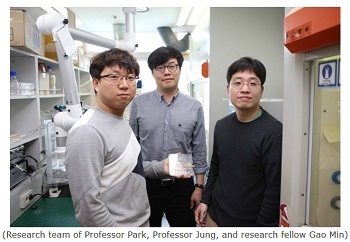
May 21, 2018 | KAISTEstimated reading time: 1 minute
A KAIST research team reported a high-performance and cost effective hydrogen sensor using novel fabrication process based on the combination of polystyrene nanosphere lithography and semiconductor microfabrication processes.
The research team, led by Professor Inkyu Park in the Department of Mechanical Engineering and Professor Yeon Sik Jung in the Department of Materials Science and Engineering, fabricated a nanostructured high-performance hydrogen gas sensor based on a palladium-decorated silicon nanomesh structure made using a polystyrene nanosphere self-assembly method. Their study was featured as the front cover article of journal “Small” (Publisher: Wiley-VCH) on March 8, 2018.
The nanosphere lithography method utilizes the self-assembly of a nanosphere monolayer. This could be an alternative choice for achieving uniform and well-ordered nanopatterns with minimum sub-10 nanometer dimensions. The research team said that the small dimensions of the silicon enhanced the palladium-gating effect and thus dramatically improved the sensitivity.
Hydrogen gas is widely considered to be one of the most promising next-generation energy resources. Also, it is a very important material for various industrial applications such as hydrogen-cooled systems, petroleum refinement, and metallurgical processes. However, hydrogen, which is highly flammable, is colorless and odorless and thus difficult to detect with human senses. Therefore, developing hydrogen gas sensors with high sensitivity, fast response, high selectivity, and good stability is of significant importance for the rising hydrogen economy.
Silicon nanowire-based devices have been employed as efficient components in high-performance sensors for detecting gases and other chemical and biological components. Since the nanowires have a high surface-to-volume ratio, they respond more sensitively to the surrounding environment.
The research team’s gas sensor shows dramatically improved hydrogen gas sensitivity compared with a silicon thin film sensor without nanopatterns. Furthermore, a buffered oxide etchant (BOE) treatment of the silicon nanomesh structure results in an additional performance improvement through suspension of nanomesh strutures from the substrate and surface roughening. The sensor device shows a fast hydrogen response (response time < 5 seconds) and 10 times higher selectivity to hydrogen gas among other gases. Their sensing performance is stable and shows repeatable responses in both dry and high-humidity ambient environments.
Professor Park said that his approach will be very useful for the fabrication of low-cost, high-performance sensors for chemical and biological detection with applications to mobile and wearable devices in the coming era of internet of things (IoTs).
Share on:


Testimonial
"In a year when every marketing dollar mattered, I chose to keep I-Connect007 in our 2025 plan. Their commitment to high-quality, insightful content aligns with Koh Young’s values and helps readers navigate a changing industry. "
Brent Fischthal - Koh YoungSuggested Items
PC Graphics Add-in Board Shipments Up 27% QoQ in 2Q25
09/03/2025 | Jon Peddie ResearchAccording to a new research report from the analyst firm Jon Peddie Research, the growth of the global PC-based graphics add-in board market reached 11.6 million units in Q2'25 and desktop PC CPUs shipments increased to 21.7 million units.
PC GPU Shipments Up 8.4% in 2Q25 on Pre-Tariff Demand
09/02/2025 | Jon Peddie ResearchJon Peddie Research reports the growth of the global PC-based graphics processor unit (GPU) market reached 74.7 million units in Q2'25, and PC CPU shipments increased to 66.9 million units.
20 Years of Center Nanoelectronic Technologies (CNT) – Backbone of German Semiconductor Research Celebrates Anniversary
08/14/2025 | Fraunhofer IPMSThe Center Nanoelectronic Technologies (CNT) of the Fraunhofer Institute for Photonic Microsystems (IPMS) is celebrating its 20th anniversary this year. Since its founding in 2005, it has developed into a pillar of applied semiconductor research in Germany and Europe. With its unique research cleanroom and equipment adhering to the 300-mm wafer industry standard, CNT is unparalleled in Germany and serves as a central innovation driver for the microelectronics industry.
Q2 Client CPU Shipments Increased 8% from Last Quarter, Up 13% YoY
08/13/2025 | Jon Peddie ResearchJon Peddie Research reports that the global client CPU market expanded for two quarters in a row, and in Q2’25, it showed unseasonal growth of 7.9% from last quarter, while server CPU shipments increased 22% year over year.
FuriosaAI Closes $125M Investment Round to Scale Production of Next-Gen AI Inference Chip
07/31/2025 | BUSINESS WIREFuriosaAI, a semiconductor company building a new foundation for AI compute, today announced it has completed a $125 million Series C bridge funding round. The investment continues a period of significant momentum for Furiosa as global demand for high-performance, efficient AI infrastructure soars.