


 Trouble in Your Tank: Implementing Direct Metallization in Advanced Substrate Packaging
 It’s Only Common Sense: Storytelling That Sells—Stop Pitching, Start Painting Pictures
 The Right Approach: Get Ready for ISO 9001 Version 6


Leveraging Imperfections to Create Better-Behaved Quantum Dots
May 23, 2018 | University of Wisconsin-MadisonEstimated reading time: 2 minutes
Potentially paving the way toward advanced computers, lasers or optical devices, University of Wisconsin-Madison researchers have revealed new effects in tiny electronic devices called quantum dots.
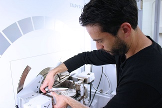
Image caption: Postdoctoral scholar Anastasios Pateras adjust an X-Ray instrument used to detect previously unknown defects in quantum dots. Photo credit: Sam Million-Weaver.
The researchers developed and applied analysis methods that will help answer other challenging questions for developing electronic materials.
“We can now look at a set of structures that people couldn’t look at before,” says Paul Evans, professor of materials science and engineering at UW-Madison. “In these structures, there are new sets of crucial materials problems that we previously weren’t able to think about solving.”
The structures Evans and colleagues looked at are thousands of times narrower than single sheets of paper, and smaller than the dimensions of individual human cells. In those structures, quantum dots form inside very thin stacks of crystalline materials topped by an asymmetrical arrangement of flat, spindly, fingerlike metallic electrodes. Between the tips of those metallic fingers are small spaces that contain quantum dots.
Creating such precise structures and peering inside those tiny spaces is technically challenging, however, and quantum dots don’t always behave as expected.
Previous work by Evans’ collaborators at the Delft University of Technology in the Netherlands, who created and extensively studied the crystal stack structures, led to suspicions that the quantum dots were different in important ways from what had been designed.
Until now, measuring those differences wasn’t possible.“Previous imaging approaches and the modeling weren’t allowing people to structurally characterize quantum dot devices at this tiny scale,” says Anastasios Pateras, a postdoctoral scholar in Evans’ group and the paper’s first author.
Pateras and colleagues pioneered a strategy for using beams of very tightly focused X-rays to characterize the quantum dot devices—and that hinged on a new method for interpreting how the X-rays scattered. Using their approach, they observed shifts in the spacing and orientation of atomic layers within the quantum dots.
“Quantum dots need to be close to perfect,” says Evans. “This small deviation from perfection is important.”
The team’s discovery indicates that the process of creating the quantum dots—laying down metallic electrodes atop a lab-grown crystal—distorts the material underneath slightly. This puckering creates strain in the material, leading to small distortions in the quantum dots. Understanding and exploiting this effect could help researchers create better-behaved quantum dots.
“Once you know these quantities, then you can design devices that take into account that structure,” says Evans.
Designs with those small imperfections in mind will be especially important for future devices where many thousands of quantum dots must all work together.
“This is going to be very relevant because, right now, there are multiple sources of decoherence quantum dots,” says Pateras.
The researchers now are developing an algorithm to automatically visualize atomic positions in crystals from X-ray scattering patterns, given that performing the necessary calculations by hand would likely be too time-consuming. Additionally, they are exploring how the techniques could add insight to other hard-to study structures.
Share on:


Testimonial
"In a year when every marketing dollar mattered, I chose to keep I-Connect007 in our 2025 plan. Their commitment to high-quality, insightful content aligns with Koh Young’s values and helps readers navigate a changing industry. "
Brent Fischthal - Koh YoungSuggested Items
MEMS & Imaging Sensors Summit to Spotlight Sensing Revolution for Europe’s Leadership
09/11/2025 | SEMIIndustry experts will gather November 19-20 at the SEMI MEMS & Imaging Sensors Summit 2025 to explore the latest breakthroughs in AI-driven MEMS and imaging optimization, AR/VR technologies, and advanced sensor solutions for critical defence applications.
Direct Imaging System Market Size to Hit $4.30B by 2032, Driven by Increasing Demand for High-Precision PCB Manufacturing
09/11/2025 | Globe NewswireAccording to the SNS Insider, “The Direct Imaging System Market size was valued at $2.21 Billion in 2024 and is projected to reach $4.30 Billion by 2032, growing at a CAGR of 8.68% during 2025-2032.”
I-Connect007’s Editor’s Choice: Five Must-Reads for the Week
07/04/2025 | Marcy LaRont, I-Connect007For our industry, we have seen several bullish market announcements over the past few weeks, including one this week by IDC on the massive growth in the global server market. We’re also closely watching global trade and nearshoring. One good example of successful nearshoring is Rehm Thermal Systems, which celebrates its 10th anniversary in Mexico and the official opening of its new building in Guadalajara.
Driving Innovation: Direct Imaging vs. Conventional Exposure
07/01/2025 | Simon Khesin -- Column: Driving InnovationMy first camera used Kodak film. I even experimented with developing photos in the bathroom, though I usually dropped the film off at a Kodak center and received the prints two weeks later, only to discover that some images were out of focus or poorly framed. Today, every smartphone contains a high-quality camera capable of producing stunning images instantly.
United Electronics Corporation Advances Manufacturing Capabilities with Schmoll MDI-ST Imaging Equipment
06/24/2025 | United Electronics CorporationUnited Electronics Corporation has successfully installed the advanced Schmoll MDI-ST (XL) imaging equipment at their advanced printed circuit board facility. This significant technology investment represents a continued commitment to delivering superior products and maintaining their position as an industry leader in precision PCB manufacturing.