


 Trouble in Your Tank: Implementing Direct Metallization in Advanced Substrate Packaging
 It’s Only Common Sense: Storytelling That Sells—Stop Pitching, Start Painting Pictures
 The Right Approach: Get Ready for ISO 9001 Version 6


Understanding the Generation of Light-Induced Electrical Current in Atomically Thin Nanomaterials
May 23, 2018 | Brookhaven National LaboratoryEstimated reading time: 5 minutes
Scientists at the Center for Functional Nanomaterials (CFN)—a U.S. Department of Energy (DOE) Office of Science User Facility at Brookhaven National Laboratory—have used an optoelectronic imaging technique to study the electronic behavior of atomically thin nanomaterials exposed to light.
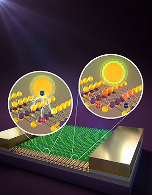
Image caption: A field-effect transistor (the device) containing molybdenum disulfide (stick and balls) doped with core-only quantum dots undergoing charge transfer (left zoom; charge transfer is shown as sparks) and core/shell quantum dots undergoing energy transfer (right zoom; energy transfer is shown as a wave moving from the quantum dots to molybdenum disulfide).
Combined with nanoscale optical imaging, this scanning photocurrent microscopy technique provides a powerful tool for understanding the processes affecting the generation of electrical current (photocurrent) in these materials. Such an understanding is key to improving the performance of solar cells, optical sensors, light-emitting diodes (LEDs), and other optoelectronics—electronic devices that rely on light-matter interactions to convert light into electrical signals or vice versa.
“Anyone who wants to know how light-induced electrical current is distributed across a semiconductor will benefit from this capability,” said CFN materials scientist Mircea Cotlet, co-corresponding author on the May 17 Advanced Functional Materials paper describing the work.
Generating an electrical current
When hit with light, semiconductors (materials that have an electrical resistance in between that of metals and insulators) generate an electric current. Semiconductors that consist of one layer or a few layers of atoms—for example, graphene, which has a single layer of carbon atoms—are of particular interest for next-generation optoelectronics because of their sensitivity to light, which can controllably alter their electrical conductivity and mechanical flexibility. However, the amount of light that atomically thin semiconductors can absorb is limited, thus limiting the materials’ response to light.
To enhance the light-harvesting properties of these two-dimensional (2D) materials, scientists add tiny (10–50 atoms in diameter) semiconducting particles called quantum dots in the layer(s). The resulting “hybrid” nanomaterials not only absorb more light but also have interactions occurring at the interface where the two components meet. Depending on their size and composition, the light-excited quantum dots will transfer either charge or energy to the 2D material. Knowing how these two processes influence the photocurrent response of the hybrid material under different optical and electrical conditions—such as the intensity of the incoming light and applied voltage—is important to designing optoelectronic devices with properties tailored for particular applications.
“Photodetectors sense an extremely low level of light and convert that light into an electrical signal,” explained Cotlet. “On the other hand, photovoltaic devices such as solar cells are made to absorb as much light as possible to produce an electrical current. In order to design a device that operates for photodetection or photovoltaic applications, we need to know which of the two processes—charge or energy transfer—is beneficial.”
(Left to right) Mingxing Li, Mircea Cotlet, Chang-Yong Nam, and Percy Zahl at the new scanning photocurrent microscopy facility at Brookhaven Lab's Center for Functional Nanomaterials.
Page 1 of 2
Share on:


Testimonial
"The I-Connect007 team is outstanding—kind, responsive, and a true marketing partner. Their design team created fresh, eye-catching ads, and their editorial support polished our content to let our brand shine. Thank you all! "
Sweeney Ng - CEE PCBSuggested Items
I-Connect007 Launches Advanced Electronics Packaging Digest
09/15/2025 | I-Connect007I-Connect007 is pleased to announce the launch of Advanced Electronics Packaging Digest (AEPD), a new monthly digital newsletter dedicated to one of the most critical and rapidly evolving areas of electronics manufacturing: advanced packaging at the interconnect level.
Panasonic Industry will Double the Production Capacity of MEGTRON Multi-layer Circuit Board Materials Over the Next Five Years
09/15/2025 | Panasonic Industry Co., Ltd.Panasonic Industry Co., Ltd., a Panasonic Group company, announced plans for a major expansion of its global production capacity for MEGTRON multi-layer circuit board materials today. The company plans to double its production over the next five years to meet growing demand in the AI server and ICT infrastructure markets.
Trouble in Your Tank: Implementing Direct Metallization in Advanced Substrate Packaging
09/15/2025 | Michael Carano -- Column: Trouble in Your TankDirect metallization systems based on conductive graphite are gaining popularity throughout the world. The environmental and productivity gains achievable with this process are outstanding. Direct metallization reduces the costs of compliance, waste treatment, and legal issues related to chemical exposure. A graphite-based direct plate system has been devised to address these needs.
Fresh PCB Concepts: Designing for Success at the Rigid-flex Transition Area
08/28/2025 | Team NCAB -- Column: Fresh PCB ConceptsRigid-flex PCBs come in all shapes and sizes. Manufacturers typically use fire-retardant, grade 4 (FR-4) materials in the rigid section and flexible polyimide materials in the flex region. Because of the small size, some rigid-flex PCBs, like those for hearing aid devices, are among the most challenging to manufacture. However, regardless of its size, we should not neglect the transition area between the rigid and flexible material.
Global Sourcing Spotlight: How to Evaluate Supplier Capabilities Worldwide
08/20/2025 | Bob Duke -- Column: Global Sourcing SpotlightIn global sourcing, the difference between a competitive edge and a catastrophic disruption often comes down to how well you vet your suppliers. Sourcing advanced PCBs, precision components, or materials for complex assemblies demands diligence, skepticism, and more than a little time on airplanes. Here’s how to do your due diligence when evaluating international suppliers and why cutting corners can cost you more than money.