


 Trouble in Your Tank: Organic Addition Agents in Electrolytic Copper Plating
 Marcy’s Musings: Can You Hear the Voices?
 Facing the Future: Successfully Navigating the Uncertain Path Ahead


Designer Materials with Completely Random Structures Might Enable Quantum Computing
June 5, 2018 | Aalto UniversityEstimated reading time: 1 minute
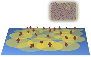
Designing quantum materials with exotic and unprecedented electrical properties has the field of physics teeming with buzz. Researchers at Aalto University in Finland have now introduced a significant turn in this discussion by developing an amorphous material which exhibits topological superconductivity. Until this point, these materials have required highly regular structures to show desired electrical properties.
The findings, published in Nature Communications, bring the field one step closer to application. Topological superconductors and insulators are considered to be possible building blocks of lossless components for quantum computers. While topological superconductors might not exist in nature, they can be fabricated, as the study demonstrates.
‘We have presented a method of fabricating topological materials in amorphous systems with randomly placed constituents. This means we can achieve superconductivity in the material by sprinkling magnetic atoms on a superconducting surface completely at random, not in highly-defined and ornamented lattices, for example,’ explains doctoral student Kim Pöyhönen.
The recent boom on topological superconductors stems mainly from an unconventional quantum-level phenomenon, a collective movement of many individual particles called Majorana fermion excitations. They have been envisioned as critical ingredients of topological quantum computers.
‘Getting highly irregular, random systems to work as topological superconductors will potentially make their fabrication and manufacture much more convenient compared to current methods,’ says research group leader, Docent Teemu Ojanen.
Perhaps for now, the implications of the random quantum material verge only on fundamental research, but that might not be the case for much longer.
‘For topological quantum matter to find its way to actual applications, it’s imperative we find even more new candidates for amorphous topological materials,’ states Ojanen.
Share on:


Suggested Items
DuPont Announces Additional Directors for the Planned Independent Electronics Company
04/18/2025 | DuPontDuPont announced that Karin De Bondt and Anne Noonan will become members of the future board of directors for the independent Electronics public company that will be created following its intended spin-off from DuPont, which is targeted for November 1, 2025.
Indium Experts to Present on Power Electronics at PCIM Europe 2025
04/17/2025 | Indium CorporationAs one of the leading materials providers to the power electronics assembly and e-Mobility industries, Indium Corporation experts will share their technical insight and knowledge on a variety of industry-related topics throughout PCIM Europe, May 6-8, in Nuremberg, Germany.
YINCAE to Showcase Cutting-Edge Solutions at SEMICON Southeast Asia 2025
04/16/2025 | YINCAEYINCAE Advanced Materials, a leading provider of innovative solutions for the semiconductor and microelectronics industries, is proud to announce its participation in SEMICON Southeast Asia 2025.
Improve Your Process Reliability: Axxon-Mycronic and HumiSeal to Host Conformal Coating Workshop in Guadalajara
04/15/2025 | Axxon-MycronicAxxon-Mycronic, a leading, global supplier of innovative and production-ready, dispensing and conformal coating systems, in collaboration with HumiSeal, a global expert in protective coating materials, is excited to announce a Conformal Coating Workshop taking place on May 8, 2025 in Guadalajara, Mexico.
Real Time with... IPC APEX EXPO 2025: Exploring LCP Materials with Matrix Electronics
04/15/2025 | Real Time with...IPC APEX EXPONolan Johnson introduces Robert Berg from Matrix Electronics, highlighting the company's focus on high-speed, low-loss flexible materials, especially LCP materials. LCP (liquid crystal polymer) is a thermal plastic with unique properties that make it ideal for advanced PCB applications. Despite processing challenges, its stability and FDA approval for medical use drive interest in aerospace and medical markets.