


 Facing the Future: Challenges and Opportunities in Reshoring PCB Manufacturing
 It’s Only Common Sense: Stop Chasing New Customers and Start Keeping the Ones You Have
 Driving Innovation: Inner Layer Alignment Methods in PCB Production


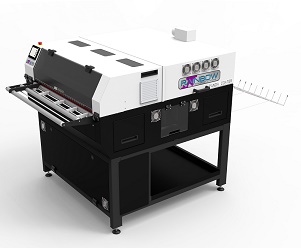
Rainbow Technology Systems Investing in Fine-Line Technology
June 18, 2018 | Rainbow Technology SystemsEstimated reading time: 2 minutes
Rainbow Technology Systems, based in Scotland, recently celebrated its 10-year anniversary. Throughout this time the company has maintained a focus on investment in the development of chemistry and equipment to enhance the manufacture of fine line circuits. This has seen the introduction to the market of the Rainbow Coating Line and Rainbow Etch Resist, making it possible to efficiently manufacture circuits in finer detail—repeatable sub-50-micron track and gap—in a small production area using minimum energy.
The Rainbow Panda Line enables artworks to be permanently coated with an ultra-thin layer of Rainbow Phototool Protect Coat to deliver significantly increased repeatability of perfect fine line imaging from one phototool.
As demand to include more functionality into ever smaller packaging grows, the challenges for high-yield production of fine line circuits intensify. These include the handling and the processing of materials and parts. Rainbow Technology are committed to being at the cutting edge of fine line production and have added further expertise and experience to their product offerings. Today, the company continues to invest further in fine line technology with the development of the Rainbow Singulation Line. This line receives a copper panel, coats the panel with a UV-curable solvent-free proprietary wet etch resist and laminates the panel with thin mylar ready for imaging with direct image systems including LDI. A horizontal flow enables the process to be installed in-line.
Airborne contamination, along with contamination inherent in materials and material processing, presents continual challenges to meeting yield targets for the manufacture of fine line circuits. In recognition of this, Rainbow Technology have acquired KSM Superclean, a leader in contact cleaning technologies. KSM’s portfolio of products permanently remove surface contamination from a wide range of materials used in critical processes for fine line manufacture to include imaging, laminating, printing and inspection. Since the acquisition, Rainbow Technology have implemented new branding and substantial enhancements to the KSM product range in terms of functionality, efficiency and design—all of which deliver increased value to customers.
David Westwood, sales & marketing manager of Rainbow Technology Systems, said: “With the commercial and technical backing of Rainbow, the KSM Superclean brand is now positioned to be an even greater force in contact cleaning. Our team has decades of experience in this sector on a global basis across many industries. Our product spectrum ranges from the manufacture of custom-made contact cleaning equipment to the supply of the highest quality consumables. We continue to innovate the fundamental characteristics of our products to deliver increased operational efficiencies and performance.”
He added: “Rainbow Technology is enjoying major growth in multiple market sectors across a broad range of products and services. This growth is enabling us to invest further in our program of development for fine line circuit manufacture, and we have some extremely interesting technologies in process. A huge factor in this is being able to call on Rainbow’s extensive in-house expertise in PCB manufacture and chemistry.”
For further information about Rainbow and KSM please click here.
Share on:


Testimonial
"In a year when every marketing dollar mattered, I chose to keep I-Connect007 in our 2025 plan. Their commitment to high-quality, insightful content aligns with Koh Young’s values and helps readers navigate a changing industry. "
Brent Fischthal - Koh YoungSuggested Items
MKS’ Atotech to Participate in IPCA Electronics Expo 2025
08/11/2025 | AtotechMKS Inc., a global provider of enabling technologies that transform our world, announced that its strategic brands ESI® (laser systems) and Atotech® (process chemicals, equipment, software, and services) will showcase their latest range of leading manufacturing solutions for printed circuit board (PCB) and package substrate manufacturing at the upcoming 17th IPCA Show to be held at Pragati Maidan, New Delhi from August 21-23, 2025.
MKS Showcases Next-generation PCB Manufacturing Solutions at the Thailand Electronics Circuit Asia 2025
08/06/2025 | MKS Instruments, Inc.MKS Inc, a global provider of enabling technologies that transform our world, today announced its participation in Thailand Electronics Circuit Asia 2025 (THECA 2025), taking place August 20–22 at BITEC in Bangkok.
Point2 Technology, Foxconn Interconnect Technology Partner to Revolutionize AI Cluster Scalability with Terabit-Speed Interconnect
08/06/2025 | BUSINESS WIREPoint2 Technology, a leading provider of ultra-low-power, low-latency mixed-signal SoC solutions for multi-terabit interconnect, and Foxconn Interconnect Technology (FIT), a global leader in precision interconnect solutions, have signed a Memorandum of Understanding (MOU) to accelerate the commercialization of next-generation Active RF Cable (ARC) and Near Pluggable e-Tube (NPE) solutions.
Advancing Electrolytic Copper Plating for AI-driven Package Substrates
08/05/2025 | Dirk Ruess and Mustafa Oezkoek, MKS’ AtotechThe rise of artificial intelligence (AI) applications has become a pivotal force driving growth in the server industry. Its challenging requirements for high-frequency and high-density computing are leading to an increasing demand for development of advanced manufacturing methods of package substrates with finer features, higher hole densities, and denser interconnects. These requirements are essential for modern multilayer board (MLB) designs, which play a critical role in AI hardware. However, these intricate designs introduce considerable manufacturing complexities.
Statement from the Global Electronics Association on the July 2025 Tariff on Copper Foil and Electronics-Grade Copper Inputs
07/31/2025 | Global Electronics AssociationWe are disappointed by today’s decision to impose a 50% tariff on imported copper foil and other essential materials critical to electronics manufacturing in the United States.