


 Trouble in Your Tank: Implementing Direct Metallization in Advanced Substrate Packaging
 It’s Only Common Sense: Storytelling That Sells—Stop Pitching, Start Painting Pictures
 The Right Approach: Get Ready for ISO 9001 Version 6


Graphene Assembled Film Shows Higher Thermal Conductivity Than Graphite Film
June 21, 2018 | CHALMERS UNIVERSITY OF TECHNOLOGYEstimated reading time: 2 minutes
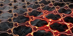
Researchers at Chalmers University of Technology, Sweden, have developed a graphene assembled film that has over 60% higher thermal conductivity than graphite film—despite the fact that graphite simply consists of many layers of graphene. The graphene film shows great potential as a novel heat spreading material for form-factor driven electronics and other high power-driven systems.
Until now, scientists in the graphene research community have assumed that graphene assembled film cannot have higher thermal conductivity than graphite film. Single layer graphene has a thermal conductivity between 3500 and 5000 W/mK. If you put two graphene layers together, then it theoretically becomes graphite, as graphene is only one layer of graphite.
Today, graphite films, which are practically useful for heat dissipation and spreading in mobile phones and other power devices, have a thermal conductivity of up to 1950 W/mK. Therefore, the graphene-assembled film should not have higher thermal conductivity than this.
Research scientists at Chalmers University of Technology have recently changed this situation. They discovered that the thermal conductivity of graphene assembled film can reach up to 3200 W/mK, which is over 60 percent higher than the best graphite films.
Professor Johan Liu and his research team have done this through careful control of both grain size and the stacking orders of graphene layers. The high thermal conductivity is a result of large grain size, high flatness, and weak interlayer binding energy of the graphene layers. With these important features, phonons, whose movement and vibration determine the thermal performance, can move faster in the graphene layers rather than interact between the layers, thereby leading to higher thermal conductivity.
“This is indeed a great scientific break-through, and it can have a large impact on the transformation of the existing graphite film manufacturing industry”, says Johan Liu.
Furthermore, the researchers discovered that the graphene film has almost three times higher mechanical tensile strength than graphite film, reaching 70 MPa.
“With the advantages of ultra-high thermal conductivity, and thin, flexible, and robust structures, the developed graphene film shows great potential as a novel heat spreading material for thermal management of form-factor driven electronics and other high power-driven systems”, says Johan Liu.
As a consequence of never-ending miniaturisation and integration, the performance and reliability of modern electronic devices and many other high-power systems are greatly threatened by severe thermal dissipation issues.
“To address the problem, heat spreading materials must get better properties when it comes to thermal conductivity, thickness, flexibility and robustness, to match the complex and highly integrated nature of power systems”, says Johan Liu. “Commercially available thermal conductivity materials, like copper, aluminum, and artificial graphite film, will no longer meet and satisfy these demands.”
The IP of the high-quality manufacturing process for the graphene film belongs to SHT Smart High Tech AB, a spin-off company from Chalmers, which is going to focus on the commercialisation of the technology.
Share on:


Testimonial
"Advertising in PCB007 Magazine has been a great way to showcase our bare board testers to the right audience. The I-Connect007 team makes the process smooth and professional. We’re proud to be featured in such a trusted publication."
Klaus Koziol - atgSuggested Items
Trouble in Your Tank: Implementing Direct Metallization in Advanced Substrate Packaging
09/15/2025 | Michael Carano -- Column: Trouble in Your TankDirect metallization systems based on conductive graphite are gaining popularity throughout the world. The environmental and productivity gains achievable with this process are outstanding. Direct metallization reduces the costs of compliance, waste treatment, and legal issues related to chemical exposure. A graphite-based direct plate system has been devised to address these needs.
Closing the Loop on PCB Etching Waste
09/09/2025 | Shawn Stone, IECAs the PCB industry continues its push toward greener, more cost-efficient operations, Sigma Engineering’s Mecer System offers a comprehensive solution to two of the industry’s most persistent pain points: etchant consumption and rinse water waste. Designed as a modular, fully automated platform, the Mecer System regenerates spent copper etchants—both alkaline and acidic—and simultaneously recycles rinse water, transforming a traditionally linear chemical process into a closed-loop system.
Driving Innovation: Depth Routing Processes—Achieving Unparalleled Precision in Complex PCBs
09/08/2025 | Kurt Palmer -- Column: Driving InnovationIn PCB manufacturing, the demand for increasingly complex and miniaturized designs continually pushes the boundaries of traditional fabrication methods, including depth routing. Success in these applications demands not only on robust machinery but also sophisticated control functions. PCB manufacturers rely on advanced machine features and process methodologies to meet their precise depth routing goals. Here, I’ll explore some crucial functions that empower manufacturers to master complex depth routing challenges.
Trouble in Your Tank: Minimizing Small-via Defects for High-reliability PCBs
08/27/2025 | Michael Carano -- Column: Trouble in Your TankTo quote the comedian Stephen Wright, “If at first you don’t succeed, then skydiving is not for you.” That can be the battle cry when you find that only small-diameter vias are exhibiting voids. Why are small holes more prone to voids than larger vias when processed through electroless copper? There are several reasons.
The Government Circuit: Navigating New Trade Headwinds and New Partnerships
08/25/2025 | Chris Mitchell -- Column: The Government CircuitAs global trade winds continue to howl, the electronics manufacturing industry finds itself at a critical juncture. After months of warnings, the U.S. Government has implemented a broad array of tariff increases, with fresh duties hitting copper-based products, semiconductors, and imports from many nations. On the positive side, tentative trade agreements with Europe, China, Japan, and other nations are providing at least some clarity and counterbalance.