


 Trouble in Your Tank: Implementing Direct Metallization in Advanced Substrate Packaging
 It’s Only Common Sense: Storytelling That Sells—Stop Pitching, Start Painting Pictures
 The Right Approach: Get Ready for ISO 9001 Version 6


Interaction of Paired and Lined-Up Electrons can Be Manipulated in Semiconductors
June 21, 2018 | Purdue UniversityEstimated reading time: 1 minute
The way that electrons paired as composite particles or arranged in lines interact with each other within a semiconductor provides new design opportunities for electronics, according to recent findings in Nature Communications.
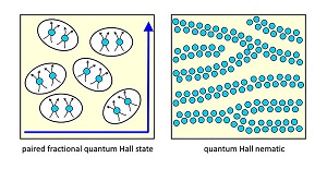
Image caption: Two different kinds of electron arrangements in a semiconductor, paired as composite particles or lined-up, can interact with and tweak each other in the presence of hydrostatic pressure. (Purdue University image/Gábor Csáthy)
What this means for semiconductor components, such as those that send information throughout electronic devices, is not yet clear, but hydrostatic pressure can be used to tune the interaction so that electrons paired as composite particles switch between paired, or "superconductor-like," and lined-up, or "nematic," phases. Forcing these phases to interact also suggests that they can influence each other's properties, like stability – opening up possibilities for manipulation in electronic devices and quantum computing.
"You can literally have hundreds of different phases of electrons organizing themselves in different ways in a semiconductor," said Gábor Csáthy, Purdue professor of physics and astronomy. "We found that two in particular can actually talk to each other in the presence of hydrostatic pressure."
Csáthy's group discovered that hydrostatic pressure, which is 10,000 times stronger than ambient pressure, compresses the lattice of atoms in a semiconductor and, therefore, influences the electron arrangement within a two-dimensional electron gas hosted by the semiconductor. The strength of the pressure determines which arrangement is favored and tunes the transition between the paired and lined-up phases, making them more tailorable for an application. Of the two phases, the paired phase may support a certain type of quantum computing.
"We can also tune the interaction by engineering the semiconductor," Csáthy said. "Say, for example, we grew a semiconductor with a particular width and electron density that we estimated could stabilize the nematic phase. Then we've tuned the electron-electron interaction as a result."
Michael Manfra, Purdue professor of physics and astronomy, electrical and computer engineering and materials engineering, and researchers Loren Pfeiffer and Kenneth West at Princeton University grew the semiconductor samples for this study. Yuli Lyanda-Geller, Purdue associate professor of physics and astronomy, provided theoretical support for the understanding on how these electron-electron interactions took place.
This research was supported by the U.S. Department of Energy, the National Science Foundation and various fellowships.
Share on:


Testimonial
"In a year when every marketing dollar mattered, I chose to keep I-Connect007 in our 2025 plan. Their commitment to high-quality, insightful content aligns with Koh Young’s values and helps readers navigate a changing industry. "
Brent Fischthal - Koh YoungSuggested Items
Global Interposer Market to Surge Nearly Fivefold by 2034
09/15/2025 | I-Connect007 Editorial TeamRevenue for the global interposer market is projected to climb from $471 million in 2025 to more than $2.3 billion by 2034, according to a new report from Business Research Insights. The growth represents a CAGR of nearly 20 percent over the forecast period.
Zhen Ding Drives AI-Powered Digital Transformation
09/12/2025 | Zhen DingDriven by the surging demand for computing power fueled by AI, the semiconductor and PCB industries are forging closer integration, expanding their ecosystems, and pursuing shared growth. PCB has already become another NT$ trillion-dollar industry in Taiwan, growing in tandem with the semiconductor sector.
Zhen Ding Expands PCB into Semiconductors at SEMICON Taiwan 2025; Advantech Drives AI Smart Parks
09/12/2025 | Zhen DingZhen Ding Technology Holding Co., Ltd., a global leader in the PCB industry, returned to exhibit at SEMICON Taiwan 2025. Positioning itself as an industry pioneer in "PCB expanding into semiconductors," the company showcased its latest strategic layout
SkyWater Completes Acquisition of Fab 25, Expanding U.S. Pure-Play Foundry Capacity for Critical Semiconductor Technologies
09/12/2025 | SkyWaterSkyWater Technology, the trusted technology realization partner, announced that it has completed its acquisition of Infineon Technologies AG’s 200 mm semiconductor fab in Austin, Texas (“Fab 25”)
Secure Semiconductor Manufacturing Acquires Full SMT Line from Manncorp
09/11/2025 | ManncorpSecure Semiconductor Manufacturing, LLC (SSM), an American-owned company dedicated to producing secure printed wiring boards and advanced assembly solutions in the MidWest USA, today announced the acquisition of a complete surface mount technology (SMT) line from Manncorp.