


 Trouble in Your Tank: Implementing Direct Metallization in Advanced Substrate Packaging
 It’s Only Common Sense: Storytelling That Sells—Stop Pitching, Start Painting Pictures
 The Right Approach: Get Ready for ISO 9001 Version 6


No Barrier to Applications for a Remarkable 2D Material
June 25, 2018 | A*STAREstimated reading time: 1 minute
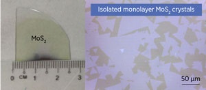
Mass production of large, uniform sheets of single-layer molybdenum disulfide, MoS2, is difficult, which limits its commercial application. A*STAR researchers have modified an existing manufacturing technique to enable the use of MoS2 in a range of technologies from photodevices to flexible, transparent sensors.
The two-dimensional material has attracted considerable attention because of its extraordinary physical, electronic and optoelectronic properties, including flexibility, transparency and semiconducting characteristics. But fabricating large-scale, defect-free single layers of MoS2 is highly challenging.
Dongzhi Chi and his team from the A*STAR Institute of Materials Research and Engineering, in collaboration with colleagues from the National University of Singapore and the Indian Institute of Science Education and Research, has modified a current technique, known as chemical vapor deposition (CVD), so that it can now produce uniform, centimeter-sized sheets of MoS2 crystals with large grain sizes.
“The physical properties of MoS2 vary greatly with its thickness,” explains Chi, “to maintain its remarkable electronic and physical properties we need a method that can uniformly deposit MoS2 films over a large area with high crystallinity.”
Although CVD is an effective technique for fabricating large-area, uniform sheets of MoS2 of varying thickness on different substrates, and significant progress has been made in improving the quality of MoS2 monolayers produced by the technique, little attention has been paid to controlling the chemical vapors using physical barriers during the growth of MoS2 crystals.
By introducing a nickel oxide (NiO) barrier, the researchers were able to control the concentration and distribution of chemical vapors during the growth of MoS2 crystals. Because NiO reacts with molybdenum trioxide (MoO3), one of the chemical reactants used in the growth process, it traps and lowers the MoO3 concentration, allowing the uniform deposition of monolayers of MoS2 over a large area.
“The advantage of this approach is the ease of implementation as well as a reduction in contamination, and it allows for control of the chemical exposure during the growth process,” says Chi.
The work has led to further advances in the fabrication of uniform and large-area MoS2 monolayers, and could also be applied to other two-dimensional materials.
“We are now looking to scale up our fabrication process for producing even larger sheets, which could pave the way for next-generation optoelectronic and sensor technologies,” says Chi.
Share on:


Testimonial
"The I-Connect007 team is outstanding—kind, responsive, and a true marketing partner. Their design team created fresh, eye-catching ads, and their editorial support polished our content to let our brand shine. Thank you all! "
Sweeney Ng - CEE PCBSuggested Items
Sustainability and Selective Soldering
09/15/2025 | Dr. Samuel J. McMaster, Pillarhouse InternationalSustainability is more than just a buzzword for the electronics industry; it’s a key goal for all manufacturing processes. This is more than a box-ticking exercise or simply doing a small part for environmentally friendly processes. Moving toward sustainable solutions drives innovation and operational efficiency.
Trouble in Your Tank: Implementing Direct Metallization in Advanced Substrate Packaging
09/15/2025 | Michael Carano -- Column: Trouble in Your TankDirect metallization systems based on conductive graphite are gaining popularity throughout the world. The environmental and productivity gains achievable with this process are outstanding. Direct metallization reduces the costs of compliance, waste treatment, and legal issues related to chemical exposure. A graphite-based direct plate system has been devised to address these needs.
EV Group Achieves Breakthrough in Hybrid Bonding Overlay Control for Chiplet Integration
09/12/2025 | EV GroupEV Group (EVG), a leading provider of innovative process solutions and expertise serving leading-edge and future semiconductor designs and chip integration schemes, today unveiled the EVG®40 D2W—the first dedicated die-to-wafer overlay metrology platform to deliver 100 percent die overlay measurement on 300-mm wafers at high precision and speeds needed for production environments. With up to 15X higher throughput than EVG’s industry benchmark EVG®40 NT2 system designed for hybrid wafer bonding metrology, the new EVG40 D2W enables chipmakers to verify die placement accuracy and take rapid corrective action, improving process control and yield in high-volume manufacturing (HVM).
Integrating Uniplate PLBCu6 With the Digital Factory Suite
09/12/2025 | Giovanni Obino and Andreas Schatz, MKS' AtotechPrinted circuit board manufacturing is rapidly changing, driven by miniaturization, stringent reliability requirements, and growing pressure for sustainable production. Meeting these challenges requires more than incremental improvements; it demands a combination of precise equipment and real-time process intelligence. The pairing of Uniplate® PLBCu6 with the Digital Factory Suite (DFS) demonstrates how hardware and software can work together to create more responsive, resource-efficient manufacturing.
Closing the Loop on PCB Etching Waste
09/09/2025 | Shawn Stone, IECAs the PCB industry continues its push toward greener, more cost-efficient operations, Sigma Engineering’s Mecer System offers a comprehensive solution to two of the industry’s most persistent pain points: etchant consumption and rinse water waste. Designed as a modular, fully automated platform, the Mecer System regenerates spent copper etchants—both alkaline and acidic—and simultaneously recycles rinse water, transforming a traditionally linear chemical process into a closed-loop system.