


 The Chemical Connection Onshoring PCB Production—Daunting but Certainly Possible
 It’s Only Common Sense: The Phone Is Still Mightier Than the Keyboard


Sintering Atomically Thin Materials with Ceramics Now Possible
June 27, 2018 | Penn State Materials Research InstituteEstimated reading time: 3 minutes
For the first time, researchers have created a nanocomposite of ceramics with a two-dimensional material that opens the door to new designs of nanocomposites with a variety of applications, such as solid-state batteries thermoelectrics, varistors, catalysts, chemical sensors and much more.
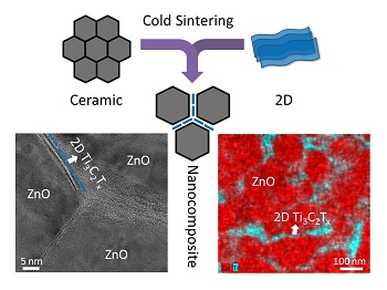
Image caption: The schematic illustration showing the co-sintering of ceramics and 2D materials using cold sintering processing, and TEM image and energy dispersive spectroscopy (EDS) map of cold sintered 99ZnO-1Ti3C2Tx nanocomposite. The MXene nanosheets are distributed homogeneously along the ZnO grain boundaries, as seen in the TEM image and EDS map. Credit: MRI/Penn State
Sintering is a method that uses high heat to compact powder materials into a solid form. Widely used in industry, ceramic powders are typically compacted at temperatures of 800 degrees Celsius or higher. Many low-dimensional materials cannot survive at those temperatures.
But a sintering process developed by a team of researchers at Penn State, called the cold sintering process (CSP), can sinter ceramics at much lower temperatures, less than 300 degrees C, saving energy and enabling a new form of material with high commercial potential.
“We have industry people who are already very interested in this work,” said Jing Guo, a post-doctoral scholar working in the group of Clive Randall, professor of materials science and engineering, Penn State. Guo is first coauthor on a paper appearing online today in the journal Advanced Materials. “They are interested in developing some new material applications with this system and, in general, using CSP to sinter nanocomposites.”
The idea of trying to develop a ceramic-2D composite system was the result of a National Science Foundation workshop on the future of ceramics, organized by Dr. Lynnette Madsen, that drew 50 of the top ceramic scientists in the U.S. Yury Gogotsi, a Charles T. and Ruth M. Bach Distinguished University Professor and Director of the A.J. Drexel Nanomaterials Institute, at Drexel University, heard Randall’s presentation on cold sintering and proposed a collaboration to develop a ceramic composite using a new class of two-dimensional materials, called MXenes, discovered by him and his collaborators at Drexel University. MXenes, which are carbide and nitride sheets a few atoms thin, possess extreme strength and many of them are excellent metallic conductors.
While it has been known that mixing even a very small amount of 2D materials, such as graphene, into a ceramic can dramatically change its properties, MXene has never been used in ceramic composites. In this work, Guo and Benjamin Legum, Gogotsi’s doctoral student, mixed 0.5-5 percent MXene into a well-known ceramic system called zinc oxide. The metallic MXene coated the ceramic powder and formed continuous two-dimensional grain boundaries, which prevented grain growth, increased the conductivity by two orders of magnitude, transforming semiconducting zinc oxide into a metallic ceramic, and doubled hardness of the final product. The addition of MXene also improved the ability of zinc oxide to transform heat to electricity.
“Ben came here quite frequently to work with Jing, and over time they overcame all of the problems involved with dispersing the 2D MXenes into the zinc oxide and then sintering it,” said Randall. “This opens a whole new world incorporating 2D materials into ceramics.”
Gogotsi added, “This is the first ceramic composite containing MXene. Taking into account that about thirty MXenes with diverse properties are already available, we are opening a new chapter in research on ceramic matrix composites, with potential applications ranging from electronics to batteries and thermoelectrics.”
Guo and Legum are co-first authors on the paper “Cold Sintered Ceramic Nanocomposites of 2D MXene and Zinc Oxide.” Gogotsi and Randall are corresponding authors. Other contributors are Dr. Babak Anasori and undergraduate student Pavel Lelukh from Drexel, and Ke Wang, staff scientist in Penn State’s Materials Research Institute.
Share on:


Testimonial
"We’re proud to call I-Connect007 a trusted partner. Their innovative approach and industry insight made our podcast collaboration a success by connecting us with the right audience and delivering real results."
Julia McCaffrey - NCAB GroupSuggested Items
ITW EAE Despatch Ovens Now Support ASTM 5423 Testing
10/15/2025 | ITW EAEAs the demand for high-performance electrical insulation materials continues to grow—driven by the rapid expansion of electric vehicles (EVs) and energy storage systems—thermal processing has become a critical step in material development.
Beyond Thermal Conductivity: Exploring Polymer-based TIM Strategies for High-power-density Electronics
10/13/2025 | Padmanabha Shakthivelu and Nico Bruijnis, MacDermid Alpha Electronics SolutionsAs power density and thermal loads continue to increase, effective thermal management becomes increasingly important. Rapid and efficient heat transfer from power semiconductor chip packages is essential for achieving optimal performance and ensuring long-term reliability of temperature-sensitive components. This is particularly crucial in power systems that support advanced applications such as green energy generation, electric vehicles, aerospace, and defense, along with high-speed computing for data centers and artificial intelligence (AI).
Is Glass Finally Coming of Age?
10/13/2025 | Nolan Johnson, I-Connect007Substrates, by definition, form the base of all electronic devices. Whether discussing silicon wafers for semiconductors, glass-and-epoxy materials in printed circuits, or the base of choice for interposers, all these materials function as substrates. While other substrates have come and gone, silicon and FR-4 have remained the de facto standards for the industry.
Creative Materials to Showcase Innovative Functional Inks for Medical Devices at COMPAMED 2025
10/09/2025 | Creative Materials, Inc.Creative Materials, a leading manufacturer of high-performance functional inks and coatings, is pleased to announce its participation in COMPAMED 2025, taking place November 17–20 in Düsseldorf, Germany.
Jiva Leading the Charge Toward Sustainable Innovation
09/30/2025 | Marcy LaRont, PCB007 MagazineEnvironmental sustainability in business—product circularity—is a high priority these days. “Circularity,” the term meant to replace “recycling,” in its simplest definition, describes a full circle life for electronic products and all their elements. The result is re-use or a near-complete reintroduction of the base materials back into the supply chain, leaving very little left for waste. For what cannot be reused productively, the ultimate hope is to have better, less harmful means of disposal and/or materials that can seamlessly and harmlessly decompose and integrate back into the natural environment. That is where Jiva and Soluboard come in.