


 The Chemical Connection Onshoring PCB Production—Daunting but Certainly Possible
 It’s Only Common Sense: The Phone Is Still Mightier Than the Keyboard


Researchers Achieve Unprecedented Control of Polymer Grids
June 28, 2018 | Northwestern UniversityEstimated reading time: 3 minutes
Synthetic polymers are ubiquitous -- nylon and polyester, Teflon and epoxy, to name just a few. All are made up of long, linear structures that can tangle. Chemists have long dreamed of making polymers with two-dimensional, grid-like formations, but this goal has proven challenging.
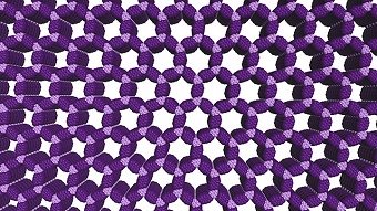
Image caption: Covalent organic frameworks (COFs) offer a unique combination of properties that show promise for waterpurification, energy storage and electronic devices.
The first examples of such structures, now known as covalent organic frameworks (COFs), were discovered in 2005, but their quality has been poor and preparation methods are uncontrolled. Now a Northwestern University research team is the first to produce high-quality versions of these materials, demonstrate their superior properties and control their growth.
The researchers developed a two-step growth process that produces organic polymers with crystalline, two-dimensional structures. The precision of the material’s structure and the empty space its hexagonal pores provide will allow scientists to design new materials with desirable properties.
Even low-quality COFs have shown preliminary promise for water purification, storing electricity, body armor and other tough composite materials. Once developed further, higher-quality samples of these materials will enable these applications to be explored more fully.
“These covalent-organic frameworks fill a century-long gap in polymer science,” said William Dichtel, an expert in organic and polymer chemistry who led the study. “Most plastics are long, linear structures that tangle up like spaghetti. We have made ordered two-dimensional polymers where the building blocks are arranged in a perfect grid of repeating hexagons. This gives us precise control of the structure and its properties.”
The 2D COFs have permanent pores and extremely high surface area. Imagine the surface area of a football field contained in about two grams of material, or two paper clips, Dichtel said. Every little hole is the same size and shape and has exactly the same composition.
In the two-step process, the scientists first grow small particle “seeds” to which they slowly add more of the building blocks, under carefully controlled conditions. The slow addition causes the building blocks to add to the seeds instead of creating new seeds. The result is larger, high-quality particles made up of large, hexagonal sheets instead of a bunch of aggregated crystals.
“This is primarily a synthesis paper, but we also measured properties that emerge only in these high-quality samples,” Dichtel said. “For example, we show that energy can move throughout the structure after it absorbs light, which may be useful in solar energy conversion.”
Once the 2D COFs were grown, fellow chemists Nathan C. Gianneschi and Lucas R. Parent carefully studied the particles using an electron microscope. They confirmed the particles are individual and not aggregated and are perfectly uniform throughout the entire structure.
Gianneschi is the Jacob and Rosaline Cohn Professor in the department of chemistry in Weinberg College. He also is a professor in the departments of materials science and engineering and of biomedical engineering in the McCormick School of Engineering. Parent is a postdoctoral fellow in Gianneschi’s group. Both are co-authors of the paper.
Next, Lin X. Chen and Richard D. Schaller measured how one of the materials interacts with light. Their studies show that energy can move through these materials for much longer distances than the sizes available through old methods.
Chen is a professor of chemistry, and Schaller is an assistant professor of chemistry, both in Weinberg. Both are co-authors of the paper.
“This study has been very gratifying -- to successfully grow these materials and begin to see their promise,” Dichtel, who has been studying COFs for a decade. “We think this development will be enabling for the field of polymer science.”
Share on:


Testimonial
"We’re proud to call I-Connect007 a trusted partner. Their innovative approach and industry insight made our podcast collaboration a success by connecting us with the right audience and delivering real results."
Julia McCaffrey - NCAB GroupSuggested Items
ITW EAE Despatch Ovens Now Support ASTM 5423 Testing
10/15/2025 | ITW EAEAs the demand for high-performance electrical insulation materials continues to grow—driven by the rapid expansion of electric vehicles (EVs) and energy storage systems—thermal processing has become a critical step in material development.
Beyond Thermal Conductivity: Exploring Polymer-based TIM Strategies for High-power-density Electronics
10/13/2025 | Padmanabha Shakthivelu and Nico Bruijnis, MacDermid Alpha Electronics SolutionsAs power density and thermal loads continue to increase, effective thermal management becomes increasingly important. Rapid and efficient heat transfer from power semiconductor chip packages is essential for achieving optimal performance and ensuring long-term reliability of temperature-sensitive components. This is particularly crucial in power systems that support advanced applications such as green energy generation, electric vehicles, aerospace, and defense, along with high-speed computing for data centers and artificial intelligence (AI).
Is Glass Finally Coming of Age?
10/13/2025 | Nolan Johnson, I-Connect007Substrates, by definition, form the base of all electronic devices. Whether discussing silicon wafers for semiconductors, glass-and-epoxy materials in printed circuits, or the base of choice for interposers, all these materials function as substrates. While other substrates have come and gone, silicon and FR-4 have remained the de facto standards for the industry.
Creative Materials to Showcase Innovative Functional Inks for Medical Devices at COMPAMED 2025
10/09/2025 | Creative Materials, Inc.Creative Materials, a leading manufacturer of high-performance functional inks and coatings, is pleased to announce its participation in COMPAMED 2025, taking place November 17–20 in Düsseldorf, Germany.
Jiva Leading the Charge Toward Sustainable Innovation
09/30/2025 | Marcy LaRont, PCB007 MagazineEnvironmental sustainability in business—product circularity—is a high priority these days. “Circularity,” the term meant to replace “recycling,” in its simplest definition, describes a full circle life for electronic products and all their elements. The result is re-use or a near-complete reintroduction of the base materials back into the supply chain, leaving very little left for waste. For what cannot be reused productively, the ultimate hope is to have better, less harmful means of disposal and/or materials that can seamlessly and harmlessly decompose and integrate back into the natural environment. That is where Jiva and Soluboard come in.