


 The Chemical Connection Onshoring PCB Production—Daunting but Certainly Possible
 It’s Only Common Sense: The Phone Is Still Mightier Than the Keyboard


New Insights Bolster Einstein’s Idea about How Heat Moves Through Solids
June 29, 2018 | ORNLEstimated reading time: 3 minutes
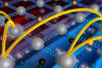
A discovery by scientists at the Department of Energy’s Oak Ridge National Laboratory supports a century-old theory by Albert Einstein that explains how heat moves through everything from travel mugs to engine parts.
The transfer of heat is fundamental to all materials. This new research, published in the journal Science, explored thermal insulators, which are materials that block transmission of heat.
“We saw evidence for what Einstein first proposed in 1911—that heat energy hops randomly from atom to atom in thermal insulators,” said Lucas Lindsay, materials theorist at ORNL. “The hopping is in addition to the normal heat flow through the collective vibration of atoms.”
The random energy hopping is not noticeable in materials that conduct heat well, like copper on the bottom of saucepans during cooking, but may be detectable in solids that are less able to transmit heat.
This observation advances understanding of heat conduction in thermal insulators and will aid the discovery of novel materials for applications from thermoelectrics that recover waste heat to barrier coatings that prevent transmission of heat.
Lindsay and his colleagues used sophisticated vibration-sensing tools to detect the motion of atoms and supercomputers to simulate the journey of heat through a simple thallium-based crystal. Their analysis revealed that the atomic vibrations in the crystal lattice were too sluggish to transmit much heat.
“Our predictions were two times lower than we observed from our experiments. We were initially baffled,” Lindsay said. “This led to the observation that another heat transfer mechanism must be at play.”
Knowing that the second heat transfer channel of random energy hopping exists will inform researchers on how to choose materials for heat management applications. This finding, if applied, could drastically reduce energy costs, carbon emissions and waste heat.
Many useful materials, such as silicon, have a chemically bonded latticework of atoms. Heat is usually carried through this lattice by atomic vibrations, or sound waves. These heat-bearing waves bump into each other, which slows the transfer of heat.
“The thallium-based material we studied has one of the lowest thermal conductivities of any crystal,” Lindsay said. “Much of the vibrating energy is confined to single atoms, and the energy then hops randomly through the crystal.”
“Both the sound waves and the heat-hopping mechanism first theorized by Einstein characterize a two-channel model, and not only in this material, but in several other materials that also demonstrate ultralow conductivity,” said ORNL materials scientist David Parker.
For now, heat-hopping may only be detectable in excellent thermal insulators. “However, this heat-hopping channel may well be present in other crystalline solids, creating a new lever for managing heat,” he said.
The study’s lead coauthor was Saikat Mukhopadhyay, a former postdoctoral research associate at ORNL and currently a National Research Council research associate at the U.S. Naval Research Laboratory.
Additional coauthors of the paper titled, “Two-channel model for ultralow thermal conductivity of crystalline Tl3VSe4,” included ORNL’s David S. Parker, Brian C. Sales, Alexander A. Puretzky, Michael A. McGuire and Lucas Lindsay.
This work was supported by the Department of Energy’s Office of Science. Raman spectroscopy measurements were made at the Center for Nanophase Materials Sciences, and the study used computational resources from the National Energy Research Scientific Computing Center at DOE’s Lawrence Berkeley National Laboratory. Both centers are DOE Office of Science User Facilities.
ORNL is managed by UT-Battelle for DOE’s Office of Science. The Office of Science is the single largest supporter of basic research in the physical sciences in the United States, and is working to address some of the most pressing challenges of our time. For more information, please click here.
Share on:


Testimonial
"Our marketing partnership with I-Connect007 is already delivering. Just a day after our press release went live, we received a direct inquiry about our updated products!"
Rachael Temple - AlltematedSuggested Items
Episode 6 of Ultra HDI Podcast Series Explores Copper-filled Microvias in Advanced PCB Design and Fabrication
10/15/2025 | I-Connect007I-Connect007 has released Episode 6 of its acclaimed On the Line with... American Standard Circuits: Ultra High Density Interconnect (UHDI) podcast series. In this episode, “Copper Filling of Vias,” host Nolan Johnson once again welcomes John Johnson, Director of Quality and Advanced Technology at American Standard Circuits, for a deep dive into the pros and cons of copper plating microvias—from both the fabricator’s and designer’s perspectives.
Nolan’s Notes: Tariffs, Technologies, and Optimization
10/01/2025 | Nolan Johnson -- Column: Nolan's NotesLast month, SMT007 Magazine spotlighted India, and boy, did we pick a good time to do so. Tariff and trade news involving India was breaking like a storm surge. The U.S. tariffs shifted India from one of the most favorable trade agreements to the least favorable. Electronics continue to be exempt for the time being, but lest you think that we’re free and clear because we manufacture electronics, steel and aluminum are specifically called out at the 50% tariff levels.
MacDermid Alpha & Graphic PLC Lead UK’s First Horizontal Electroless Copper Installation
09/30/2025 | MacDermid Alpha & Graphic PLCMacDermid Alpha Electronics Solutions, a leading supplier of integrated materials and chemistries to the electronics industry, is proud to support Graphic PLC, a Somacis company, with the installation of the first horizontal electroless copper metallization process in the UK.
Electrodeposited Copper Foils Market to Grow by $11.7 Billion Over 2025-2032
09/18/2025 | Globe NewswireThe global electrodeposited copper foils market is poised for dynamic growth, driven by the rising adoption in advanced electronics and renewable energy storage solutions.
MacDermid Alpha Showcases Advanced Interconnect Solutions at PCIM Asia 2025
09/18/2025 | MacDermid Alpha Electronics SolutionsMacDermid Alpha Electronic Solutions, a global leader in materials for power electronics and semiconductor assembly, will showcase its latest interconnect innovations in electronic interconnect materials at PCIM Asia 2025, held from September 24 to 26 at the Shanghai New International Expo Centre, Booth N5-E30